May 6 2024Reviewed by Lexie Corner
Scientists at the Department of Energy’s Oak Ridge National Laboratory have conducted research that shows how minute variations in the isotopic content of thin semiconductor materials can affect their optical and electronic characteristics. This research, which has been published in Science Advances, could potentially lead to the development of novel and cutting-edge semiconductor designs.
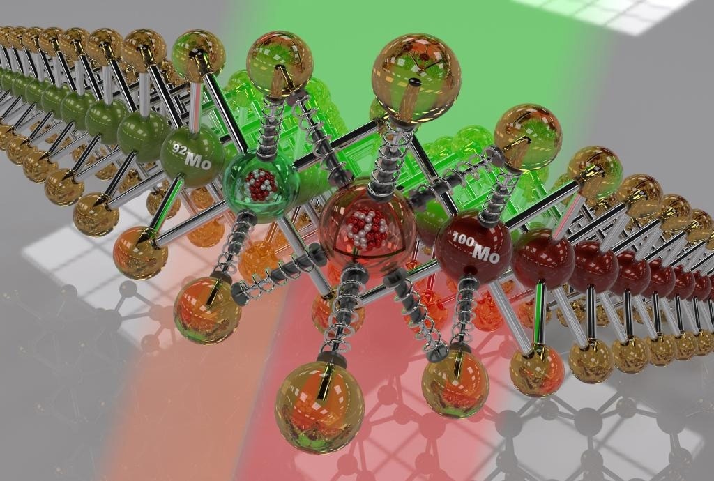 Surprisingly, changing isotope masses of molybdenum in a single layer of semiconductor molybdenum disulfide shifted the color of light emitted when the layer was illuminated. The study revealed the potential of isotope engineering to design new technologies in 2D materials. Image Credit: Chris Rouleau/ORNL, US Dept. of Energy
Electronic systems and devices become more complex and advanced every day, in part due to semiconductors. For this reason, scientists have been researching ways to enhance semiconductor compounds to affect their ability to carry electrical current. One strategy is to manipulate isotopes of material properties—physical, chemical, and technological.
Isotopes are members of an element's family that share the same number of protons but differ in mass due to differences in neutron counts. Traditionally, the goal of isotope engineering has been to improve so-called bulk materials, or 3D materials, which have uniform properties in three dimensions.
However, recent work led by ORNL has advanced the field of isotope engineering in which a layer of only a few atoms thick is confined to current in two dimensions, or 2D, inside flat crystals. The ultrathin nature of the 2D materials may enable precise control over their electrical properties, which makes them promising.
We observed a surprising isotope effect in the optoelectronic properties of a single layer of molybdenum disulfide when we substituted a heavier isotope of molybdenum in the crystal, an effect that opens opportunities to engineer 2D optoelectronic devices for microelectronics, solar cells, photodetectors, and even next-generation computing technologies.
Kai Xiao, Scientist, Oak Ridge National Laboratory
Using molybdenum atoms of various masses, Yiling Yu, a researcher on Xiao's team, created isotopically pure 2D crystals of atomically thin molybdenum disulfide. Yu saw slight changes in the color of light emitted by the crystals under photoexcitation (stimulation by light).
Unexpectedly, the light from the molybdenum disulfide with the heavier molybdenum atoms was shifted farther to the red end of the spectrum, which is opposite to the shift one would expect for bulk materials.
Kai Xiao, Scientist, Oak Ridge National Laboratory
The red shift indicates a change in the material's electronic structure or optical properties.
Working with theorists Volodymyr Turkowski and Talat Rahman at the University of Central Florida, Xiao and colleagues knew that in the confined dimensions of these ultrathin crystals, the phonons, or crystal vibrations, must be scattering the excitons, or optical excitations, in unexpected ways.
The scientists found that, for heavier isotopes, this scattering causes the optical bandgap to shift towards the red end of the light spectrum. The term “optical bandgap” describes the lowest energy required for a material to either emit or absorb light. Researchers can make semiconductors absorb or emit different colors of light by varying the bandgap, and this tunability is crucial for creating new devices.
Alex Puretzky of ORNL explained different crystals grown on a substrate can display subtle changes in the emitted color caused by regional strain within the substrate. To validate the anomalous isotope effect and assess its extent in relation to theoretical forecasts, Yu cultivated molybdenum disulfide crystals that contained two distinct molybdenum isotopes.
Xiao said, “Our work was unprecedented in that we synthesized a 2D material with two isotopes of the same element but with different masses, and we joined the isotopes laterally in a controlled and gradual manner in a single monolayer crystal. This enabled us to observe the intrinsic anomalous isotope effect on the optical properties in the 2D material without the interference caused by an inhomogeneous sample.”
The study demonstrated that even a small change of isotope masses in atomically thin 2D semiconductor materials can influence optical and electronic properties. This finding provides an important basis for continued research.
“Previously, the belief was that to make devices such as photovoltaics and photodetectors, we had to combine two different semiconductor materials to make junctions to trap excitons and separate their charges. But actually, we can use the same material and just change its isotopes to create isotopic junctions to trap the excitons. This research also tells us that through isotope engineering, we can tune the optical and electronic properties to design new applications,” said Xiao.
This work was carried out at the Center for Nanophase Materials Sciences, or CNMS, at ORNL, an Office of Science user facility, with funding from the DOE's Office of Science, Basic Energy Sciences, Materials Sciences, and Engineering Division. The measurements for optical spectroscopy, STEM, and TOF-SIMS were supported by the CNMS.
Journal Reference:
Yu, Y., et al. (2024) Anomalous isotope effect on the optical bandgap in a monolayer transition metal dichalcogenide semiconductor. Science Advances. doi.org/10.1126/sciadv.adj0758.
Source: https://www.ornl.gov/