DOI :
10.2240/azojomo0277
Apr 30 2009
A. B. Glot A, A. P. Sandoval-García B, A. V. Gaponov C, R. Bulpett D, B. J. Jones D and G. Jimenez-Santana
Copyright AD-TECH; licensee AZoM.com Pty Ltd.
This is an AZo Open Access Rewards System (AZo-OARS) article distributed under the terms of the AZo–OARS https://www.azom.com/oars.asp which permits unrestricted use provided the original work is properly cited but is limited to non-commercial distribution and reproduction.
AZojomo (ISSN 1833-122X) Volume 5 April 2009
Topics Covered
Abstract
Keywords
Introduction
Experimental
Results and Discussion
Microstructure
Current-Voltage Characteristics
Capacitance Relaxation
Conclusion
Acknowledgment
Appendix: Model of Capacitance Relaxation
References
Contact Details
Abstract
Tin dioxide based varistor ceramics SnO2-Co3O4-Nb2O5-Cr2O3-xCuO (x=0; 0.05; 0.1 and 0.5) were made and their electrical properties were studied. The highest nonlinearity coefficient and electric field (at current density 10-3 A cm-2) were obtained for 0.1 mol.% CuO addition. It was observed that low-field electrical conductivity is increased with relative humidity, therefore, materials obtained exhibit double function of varistor and humidity sensor. The highest humidity sensitivity coefficient is found for SnO2-Co3O4-Nb2O5-Cr2O3 ceramics (without CuO). Observed varistor and humidity-sensitive properties are explained in the frames of grain-boundary double Schottky barrier concept as a decrease of the barrier height with electric field or relative humidity. Using suggested simple theory and data obtained on isothermal capacitance relaxation, the energy of the grain-boundary monoenergetic trapping states were estimated. These values are less than found for activation energy of electrical conduction (as a measure of the barrier height). These observations confirm the barrier concept.
Keywords
Electrical Conduction, Grain Boundary, Humidity Sensor, SnO2 Ceramics, Varistor
Introduction
Tin dioxide (SnO2) is n-type semiconductor due to native defects and is widely used in various areas of electronics [1-15]. Particularly, applications of tin dioxide based ceramics as varistors [2, 3, 6, 8, 10, 14, 15] and as humidity sensors [5,9,11] are known. Varistors are semiconductor devices with nonlinear (super linear) dependence of current on voltage , which is the same for both voltage polarities [2, 16]. In varistors the phenomenon of non-Ohmic electrical conduction is used. Usually varistor is characterized by two empirical parameters: the nonlinearity coefficient and the electric field estimated at the current density 10-3 Acm-2. Resistive-type humidity sensors are devices with the dependence of their resistance on relative humidity [9, 11].
Tin dioxide based ceramics with additives are used for a device with combined properties of a varistor and a sensor of relative humidity [6] and varistor-type gas sensors [17,18]. Recently SnO2-Bi2O3-Co3O4-Nb2O5-Cr2O3 ceramics with high nonlinearity coefficient () and high humidity sensitivity () at low electric fields was suggested [19, 20]. The combining of both properties in SnO2-Co3O4-Nb2O5-Cr2O3-Bi2O3 varistor-sensor is due to the grain-boundary nature of both effects [19, 20]. Non-Ohmic conduction in tin dioxide based ceramics is due to a decrease of the barrier height on electric field [21]. The high sensitivity of low-field conductivity to humidity variations is due to a weak lowering of the barrier height in humid atmospheres [20].
Non-Ohmic conduction is observed in tin dioxide based ceramics with different additives [2, 3, 6, 8, 10, 14, 15, 19]. For example, for SnO2-CoO-Nb2O5-Al2O3 varistor [14] and and for SnO2-Co3O4-Nb2O5-Cr2O3 [15] varistor and were obtained. Recently it was shown that for a comparison of nonlinear properties of varistors with different values it is better to use the normalized nonlinearity coefficient [21-23]. For SnO2-Co3O4-Nb2O5-Cr2O3 [15] system is higher ( 1.03·10-2 cm·V–1) than for SnO2-CoO-Nb2O5-Al2O3 [14] system ( 3.96·10-3 cm·V-1). Therefore, choosing the base system the preference has been given to the system with Cr2O3 addition. In SnO2 - based systems with CuO addition the values of the nonlinearity coefficient (at electric field ) were reported [24-26]. However, we have found recently that in a SnO2-Co3O4-Nb2O5-Cr2O3-CuO system some higher values of the nonlinearity coefficients (about 50) at relatively not too high electric field can be reached. It would be interesting to study these materials in details and to know, in particular, if double properties of a varistor and a humidity sensor can be observed in such SnO2-Co3O4-Nb2O5-Cr2O3-CuO ceramics.
In spite of the recent findings that non-Ohmic conduction in SnO2 ceramics is related to a weak decrease of the barrier height at low electric fields and to a strong decrease of the barrier height at high electric fields [21-23] (quite similar to what was found in ZnO varistors [16]), the electronic structure of grain boundaries in tin dioxide varistor ceramics is still poorly studied. Therefore, the role of grain-boundary electronic processes (capture and emission of electrons) in the mechanism of non-ohmic conduction is not clearly understood.
It was found earlier that electrical properties of SnO2 varistors are similar to the properties of ZnO varistors and it was assumed that non-Ohmic conduction in ZnO and SnO2 varistors have a common physical nature related to the transport of electrons across the grain-boundary potential barriers [10]. This assumption was confirmed recently by the similarity of non-Ohmic conduction mechanism in ZnO and SnO2 varistors [21-23]. Using the above idea and taking into account that in ZnO-based varistors filling of the interface states at low fields prevent a sharp decrease of the barrier height [16], it can be assumed that capture of electrons at the
grain-boundary states in SnO2 based varistor ceramics is important in a stabilization of the grain-boundary barriers at low fields. For a confirmation of this hypothesis we studied isothermal capacitance relaxation. For the estimation of some parameters of the electronic grain-boundary states in ZnO varistor ceramics different methods based on a capacitance measurement are applied [27-30]. In particular, isothermal capacitance relaxation in ZnO varistors was studied [30]. Therefore, in this paper not only tin dioxide based SnO2-Co3O4-Nb2O5-Cr2O3-CuO varistor ceramics are obtained and their current-voltage characteristics in air with different relative humidity are recorded but as well as isothermal capacitance relaxation are studied with the aim to confirm an existence of grain-boundary barriers in SnO2 varistor ceramics and find the energy of electron trapping centers at the grain-boundary interface.
Experimental
The samples (mol.%) (99.4-x) SnO2-0.5Co3O4-0.05Nb2O5-0.05Cr2O3-xCuO (x=0; 0.05; 0.1 and 0.5) were prepared by conventional mixture method. Mixtures of oxides were wet-milled with distilled water and pressed into tablets 12 mm in diameter and about 0.8 mm thick under axial pressure 45 MPa. Pressed tablets were sintered in air at temperature of 1520 K (1 hour) with heating and cooling rates of about 350 K/hour. Phase compositions of the samples were studied by X-ray diffraction (XRD). Differential thermal and thermo gravimetrical analyses were performed at heating up to sintering temperature to detect possible phase transitions and mass change. Scanning electron microscopy (SEM) was used to explore the grain size and the pore size throughout the sintered sample at the as-sintered surfaces. Energy dispersive X-ray microanalysis (EDX) was applied to study local distribution of chemical elements. All electrical measurements were performed using samples with Ag-electrodes. Ag-electrodes were obtained by slow heating of a sample (with flat surfaces covered by Ag-paste) in air up to a temperature of 1070 K and slow cooling. Current-voltage characteristics were recorded in air with fixed relative humidity by applying d.c. voltage and measuring the steady-state current. Possible self heating of a sample during the measurement was detected as an increase of current at a fixed voltage.
The results were obtained avoiding the self-heating of samples. In spite of true comparison of several samples with nonlinear current-voltage dependence can be made analysing current-voltage characteristics in the whole current range, sometimes it is useful to have some empirical numerical parameters for the characterization of nonlinear behaviour of each sample. With this purpose the nonlinearity coefficient was estimated at the current density 10-3 Acm-2 as the slope of current-voltage characteristic plotted in double logarithmic scale . Electric field was obtained at the same current density. The choice of the traditional value of 10-3 Acm-2 for samples studied is because at this current the nonlinearity of current-voltage characteristics is usually quite high, therefore it is convenient to estimate the voltage applied to a device, because at this current the voltage weakly depends on the current allowing to compare different devices. This current density is accessible in dc regime for samples with typical cross-section of about 1 cm2. For a recording of current-voltage characteristic in air at fixed relative humidity in the range 10 – 93% a sample was placed in a closed chamber above the surface of water solution of a proper salt for a time of about 1 hour before starting the measurements. Humidity sensitivity coefficient was calculated at 1000 V·cm-1, W1= 10% and W2= 93%.
Time dependence of capacitance (and conductance ) were measured at fixed temperatures in the range 295-355 K at frequency 1 kHz after the application of dc voltage of 100 V during 2 minutes using 7600 precision LRC meter model B (QuadTech) in air with relative humidity approximately 50%. Measurements were performed at the samples with nearly the same thickness 0.7 mm. After 2 minutes under voltage the steady state capacitance values were observed and longer times had no effect on results. Two curves obtained at 293 K, one in air with fixed relative humidity 51% and other in air with relative humidity approximately 50%, were nearly the same. Therefore, it is assumed that humidity had no significant effect on measurements.
The energy of the grain-boundary trapping states was estimated using simple model developed in Appendix. Temperature dependence of electrical conductivity in the range of about 295-475 K was obtained by slow heating and cooling (about 1 K/min) of a sample in air with relative humidity approximately 50%. The activation energy of electrical conduction is found from high-temperature part of dependence obtained at heating according to the expression , where is the Boltzmann´s constant and is absolute temperature. Low-temperature part of dependences contains anomalous region related to non-zero relative humidity [19]. Temperature dependence of obtained at cooling gives as a rule slightly lower (about 0.1 eV) values of due to possible desorption of oxygen at such heat treatment, however, this difference is not very important for the purposes of a comparison in this paper values with lower values.
Results and Discussion
In this section microstructure and dc electrical properties of SnO2-Co3O4-Nb2O5-Cr2O3-CuO ceramics are discussed followed by the analysis of capacitance relaxation at fixed temperature after an application of dc voltage.
Microstructure
Material without the addition of CuO is not sintered completely, and many pores are seen, though there is no evidence of a secondary phase (Figure 1,a). At 0.1 mol.% CuO sintering is better (more grain boundaries without pores are appeared) though pores exist and microstructure is similar to that for sample without CuO (Figure 1,b). Some dark areas are seen as well (Figure 1,a and b). These can be explained by surface contaminations by hydrocarbons. Ceramic sample with 0.5 mol.% CuO is better sintered (Figure 1,c). Further detailed study in the SEM has revealed that the sample with 0.5 mol.% CuO has a larger grain size and also contains secondary phases at grain boundaries (Figure 1,c). In the central part of grains (Figure 1) only tin and oxygen are detected (Figure 2,a). The tin signal is larger than the oxygen signal because the efficiency is lower for low energy X-rays. Small crystalline-like inclusions are seen at some grain boundaries (highlighted ‘B’ in Figure 1,c). Figure 2,b shows EDX spectrum of such a grain boundary phase with tin, silicon, cobalt and copper. A large tin signal can be due to the analysis spot overlapping with the adjacent tin dioxide grains and silicon signal can be caused by the contact of powder with porcelain during preparation procedure.
The oxygen signal is much higher than in the grain. The intensity of EDX Co-lines obtained from these inclusions is higher than the intensity of Cu-lines (Figure 2,b). An additional phase is distributed along the grain boundaries (highlighted ‘A’ in Figure 1,c). This may be the result of the solidification of some liquid phase formed during sintering. Figure 2,c shows high levels of copper with high oxygen and lower silicon in this grain boundary phase. In these areas, the intensity of Cu-lines of the EDX spectrum is higher than the intensity of Co-lines (Figure 2,c). The existence of liquid phase at sintering temperature is supported by observation of the endothermic peak at about 1360 K (1090°C) at heating of a sample. The most preferable meaning of melting temperature of CuO is 1093-1099°C [31].
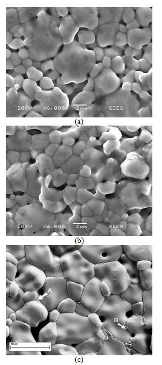
Figure 1. SEM micrographs of as-sintered surface of SnO2-Co3O4-Nb2O5-Cr2O3-CuO ceramic varistor (a) without CuO addition, (b) with an addition 0.1 mol.% CuO and (c) 0.5 mol.% CuO. Clearly visible secondary phases A and B are marked.
These temperatures are close and, therefore, probably melting of CuO takes place below the sintering temperature. The situation can be quite complicated due to possible conversion of CuO to Cu2O (the observed lost of mass can be explained by runaway of oxygen). This Cu- rich phase occurs at grain boundaries rather inhomogeneously throughout the sample. X-ray diffraction of the sample with 0.5 mol.% CuO shows only lines of tetragonal SnO2 (rutile structure) and it is the same for the sample with 8 mol.% CuO. The thermogravimetry shows the decrease of mass during heating both in sintered and in unsintered samples although in the former the mass loss is lower. Therefore, some part of CuO presumably can be evaporated during sintering and, therefore, it is difficult to detect XRD lines related to CuO. In the XRD spectrum of the sample with 50 mol.% CuO the lines of SnO2, CuO and Cu2O are seen. It suggests that CuO does not form any compound with SnO2, but rather that both CuO and Cu2O can exist in the sintered sample. Additionally, the sample with 0.5 mol.% CuO contains a small amount of Cu-Co-O phases (possibly with Sn) as seen in Figure 1,c which are not detectable by XRD.
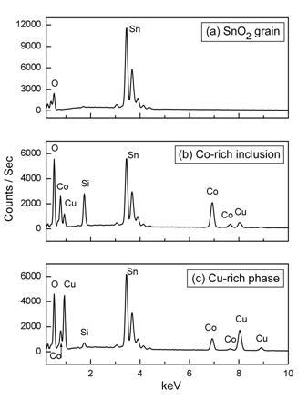
Figure 2. EDX spectra of sample with 0.5 mol.% CuO (see Figure 1,c) showing analysis of (a) SnO2 grain, (b) Co-rich crystal inclusion (indicated B in Figure 1,c) and (c) Cu-rich secondary phase (indicated A in Figure 1,c).
It is necessary to point out that formation of the grain-boundary barriers during sintering in oxidizing atmosphere depends on many factors like bulk and surface structure of SnO2 grains, mutual orientation of neighboring grains, surface electronic structure, chemisorbed oxygen, used oxide additives and others. This problem is quite complicated (see, for example, [32]) and, extends beyond the composition analysis discussed in this paper. For that reason the structure of grains and grain boundaries are not discussed in this paper.
Current-Voltage Characteristics
In Figure 3 current-voltage characteristics of SnO2-Co3O4-Nb2O5-Cr2O3-CuO ceramics with different amount of CuO are shown and they are nonlinear. The electric field strength and the nonlinearity coefficient (at 10-3 A cm-2) are presented in Table 1.
Table 1. Some parameters of SnO2-Co3O4-Nb2O5-Cr2O3-CuO ceramics.
|
CuO addition, mol.%
|
E1, V·cm-1
|
β
|
S
|
Eσ, eV
|
ET, eV
|
|
0
|
3130
|
11
|
2.75×10⁴
|
1.21
|
0.59
|
|
0.05
|
3850
|
20
|
2.3×10⁴
|
1.05
|
0.48
|
|
0.1
|
3610
|
50
|
9.9×10³
|
1.02
|
0.50
|
|
0.5
|
1940
|
8
|
4.5×10³
|
0.94
|
0.49
|
E1 is electric field obtained at the current density 10-3 A cm-2
β is the nonlinearity coefficient estimated at the current density 10-3 A cm-2
Electrical properties of SnO2 varistors [2, 6, 8, 14, 15, 19-22, 24-26] as well as ZnO varistors [16, 23, 27] are controlled by grain boundaries because in these ceramics grains are quite conductive but grain-boundary regions are resistive due to the formation of grain-boundary potential barriers during sintering in oxidizing atmosphere. High-current pulse measurements shows that grain resistivity in SnO2 varistor is about 4 Ohm·cm though low-field resistivity of ceramic sample is about 109 Ohm·cm [21]. Therefore, grains do not affect dc electrical properties of SnO2 varistors and become important only in the high-current range. The variation of small additives to SnO2 can change the conditions of barrier formation and, therefore, can change electrical properties of SnO2 varistors. The barrier formation process in SnO2 varistor ceramics can be influenced by the formation of secondary grain-boundary phases as in the case of SnO2 varistor ceramics with Bi2O3 addition [19]. A similar situation can occur in the present case of Cu addition (see Figures 1 and 2). The current-voltage characteristics of SnO2-Co3O4-Nb2O5-Cr2O3-CuO ceramics depend on the CuO amount as discussed below. The electric field is slightly changed with increase of CuO amount in the range 0.05-0.1mol.% and it is strongly decreased for 0.5 mol.% CuO (Figure 3, Table 1). At 0.5 mol.% CuO addition the grain growth is observed (Figure 1,c) and, therefore, becomes lower. Such correlation can be realized if we assume that voltage in the range of high nonlinearity for different single grain boundaries in the ceramics studied with variable amount of CuO is relatively constant. Similar situation generally takes place in ZnO varistor ceramics [16] but for SnO2 varistor ceramics this question is still open. During sintering formation of a secondary phase in the sample with 0.5 mol.% CuO can be assumed (see Figures 1 and 2). The effect of CuO addition on the low-field conductivity is not well-marked from Figure 3 possibly due to an action of some opposite factors.
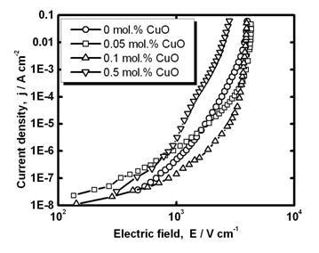
Figure 3. Current-voltage characteristics of SnO2-Co3O4-Nb2O5-Cr2O3-CuO ceramics with different amount of CuO. Measurements are performed at fixed relative humidity 51%.
On the one hand, increase of CuO addition in the range 0.05-0.1 mol.% can presumably improve the distribution of Cr2O3 throughout the sample due to the appearance of liquid phase and promote the increase of the barrier height. Then low-field conductivity can be lower. For example, an addition of Cr2O3 to SnO2–Bi2O3-Co3O4-Nb2O5 leads to an increase of the activation energy of electrical conduction from 0.87 to 1.2 eV (see [19, 21]).
On the other hand, it can be assumed that at high temperatures (above about 1300 K) both ions Cu2+ and Cu+ can exist in the Cu-rich secondary phase and on cooling after sintering the ratio Cu2+/Cu+ is increased [25]. As a result some small amount of oxygen will be bonded by copper instead of being adsorbed at the grain boundary. Therefore, the barrier height and the activation energy in ceramics with higher CuO addition can be lower and low-field conductivity respectively can be higher. At 0.5 mol.% CuO, low-field current across the grain-boundary barrier can be comparable to the current across the secondary phase. This can be responsible for observed (Figure 3) weak variation of current-voltage characteristics at low electric fields (where currents are in the range 10-8-10-6 A).
For the estimation of the grain-boundary barrier height temperature dependence of electrical conductivity was studied (Figure 4). Values obtained for the activation energy of electrical conduction are summarized in Table 1. It can be assumed that Fermi level in tin dioxide grain far from the boundary is situated about 0.1-0.2 eV below the conduction band edge [4]. Therefore, obtained values give quite correct estimation of the barrier height: . Experimental values of are decreased with CuO addition (Table 1). Therefore, the barrier height is decreased with CuO addition possibly due to an increase of the ratio Cu2+/Cu+ at cooling after sintering (see [25]).
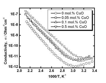
Figure 4. Temperature dependence of dc electrical conductivity in air (heating ) for SnO2-Co3O4-Nb2O5-Cr2O3-CuO varistor ceramics with different amount of CuO addition.
However, the nonlinearity coefficient (at 10-3 A cm-2) is increased with CuO addition up to 50 at 0.1 mol.% CuO but material with 0.5 mol.% CuO exhibits a low nonlinearity coefficient (Table 1). Taking into account that Cr2O3 addition is responsible for an increase of the nonlinearity in the system SnO2-Co3O4-Nb2O5-Cr2O3 [15], observed increase of with CuO addition can be explained by better distribution of Cr2O3 throughout the sample in the presence of CuO. It was shown recently that a dependence of the barrier height on voltage for single SnO2 grain boundary plays a key role in varistor effect and it determines current-voltage characteristic of a ceramic sample [21]. Then, small CuO addition together with Cr2O3 addition can promote some changes in the energy distribution of the interface (CuO, Cr2O3) and bulk (Cr2O3) states density. As a result the barrier height is decreased slightly at low fields but it is decreased more at high fields. This leads to relatively high nonlinearity of current-voltage characteristic of the sample with 0.1 mol.% CuO (Table 1). At 0.5 mol.% CuO Cu-rich secondary phase, being quite conductive, can work as a shunt to the grain boundary decreasing the nonlinearity of its current-voltage characteristic. Therefore, the nonlinearity coefficient passes the maximum with variation of CuO addition.
It was shown recently that SnO2-Bi2O3-Co3O4-Nb2O5-Cr2O3 ceramics (with Bi2O3 addition) are materials with combined properties of a varistor (at high fields) and a humidity sensor (at low fields) [19, 20]. Therefore, we decided to study current-voltage characteristics of SnO2-Co3O4-Nb2O5-Cr2O3-CuO ceramics at variable humidity conditions. It was found that all studied materials are not only non-Ohmic but humidity-sensitive. As an additional example current-voltage characteristics of the sample with 0.1 mol.% CuO in air with different relative humidity are shown in Figure 5.
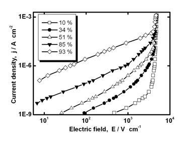
Figure 5. Current density vs. electric field for SnO2-Co3O4-Nb2O5-Cr2O3-0.1 mol.% CuO sample in air with different relative humidity.
It can be seen that the low-field electrical conductivity is increased with relative humidity, however, current-voltage characteristics are still highly nonlinear at high fields (Figure 5). Humidity sensitivity coefficient is gradually decreased with CuO addition in the range 0-0.5 mol.% (Table 1). For higher amounts of CuO addition (2, 4 and 8 mol.%) further lowering of (5.5·102, 5.5, and 1.2, respectively) is found. It is assumed that observed decrease of can be related not only to the covering of grain-boundary regions by CuO-rich phase but as well to an action of this phase as a shunt to a grain boundary. An addition of CuO can probably diminish the role of barrier-related sensitivity mechanism. Thus, obtained SnO2-Co3O4-Nb2O5-Cr2O3-CuO varistor ceramics are materials with humidity-sensitive low-field electrical conductivity. The capacitance value in barrier-controlled materials should be sensitive to the variation of voltage bias. Therefore, capacitance measurements can give an additional indication of a presence of the grain-boundary potential barriers in materials studied and parameters of these barriers can be obtained.
Capacitance Relaxation
Application of dc voltage causes rapid decrease of capacitance on time due to a capture of electrons at the grain-boundary states (Figure 6). After a decrease of dc bias to zero it slowly increased due to an emission of electrons from the grain-boundary states (Figure 6). Higher applied voltage causes stronger decrease of capacitance, therefore, after the elimination of voltage capacitance is relaxed from lower values. If we assume nearly exponential decrease of the capacitance difference on time (Figure 6), then time constants for two relaxation curves obtained after the application of different voltages (50 and 100V) are approximately equal because the same levels are filled at different voltages. Similar capacitance variation on time was observed in the explored range of temperature 290-360 K for all the samples studied.
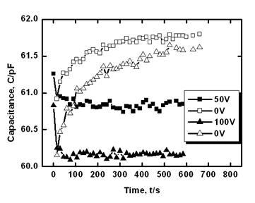
Figure 6. Time variation of capacitance of the ceramic sample without CuO addition under dc bias U=50 V, subsequent capacitance relaxation at dc bias U=0, then capacitance under dc bias U=100 V and subsequent capacitance relaxation at dc bias U=0.
This phenomenon can be realized on the basis of the model presented in the Appendix assuming that the grain-boundary barrier in tin dioxide varistors studied can be the double Schottky barrier (two Schottky barriers connected in opposite directions). Additionally, increase of dc voltage (from 50 to 100V) leads to a decrease of the steady state capacitance value (Figure 6).It can be explained by some widening of the depletion layer at the positive side of the grain boundary (reverse biased Schottky barrier layer). For the estimation of the energy of trapping level (the energy of grain-boundary states which capture electrons; this energy is calculated from the top of the barrier) capacitance relaxation curves (Figure 6, without bias) were recorded at several temperatures for each sample. Results obtained in the scale according to Eq.(A10) (see the Appendix) are presented in Figure 7.It is seen that the difference in between two samples with different amount of CuO is small. Slight decrease of the slopes of at all temperatures for the sample with 0.5 mol.% CuO in comparison to the sample without CuO (Figure 7) can be related to higher values of the relaxation time (see Eq.(A10) in the Appendix).
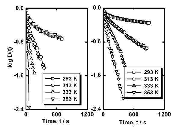
Figure 7. Time dependence of (see Eq.(A10)) at several temperatures for ceramic sample without CuO (left) and for ceramic sample with 0.5 mol.% CuO addition (right).
This is confirmed by Figure 8. Some growth of for the sample, where secondary phase exists (Figures 1 and 2), can be due to the lower coefficient of emission in Eq.(A9) (see the Appendix) though the energy is nearly the same (see Figure 8): in the case of the sample with 0.5 mol.% CuO some localized grain-boundary states can be situated in the mentioned secondary phase.
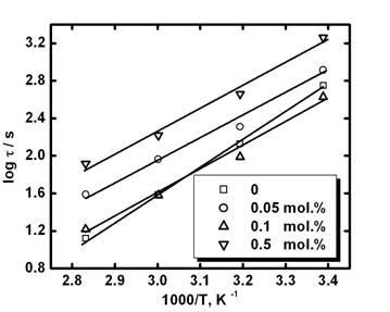
Figure 8. Temperature dependence of relaxation time for SnO2-Co3O4-Nb2O5-Cr2O3-CuO ceramics with different amount of CuO.
Electrons escape from these states slower than from grain-boundary states at the surface of SnO2 (sample without CuO addition), therefore, coefficients of emission is lower and the relaxation time (see Eq.(A9)) is higher for the sample with 0.5 mol.% CuO. In the developed model (see Appendix) secondary grain-boundary phase is absent though similar formulas are expected if to take into account such a grain-boundary phase.
It should be mentioned that experimental curves in the scale are not strictly linear. Taking into account Eq.(A10) it can be concluded that the relaxation time is slightly changed during the relaxation process.
It can be due to the energy distribution of the grain-boundary states. At the initial stage of capacitance relaxation electrons escape from more shallow states. Later electrons escape from more deep states. Using almost linear parts of curves in Figure 7 (at long times) the time constants of the emission process at several temperatures were obtained.
Temperature dependences of the relaxation time for SnO2-Co3O4-Nb2O5-Cr2O3-CuO ceramics with different amount of CuO are shown in Figure 8. In Table 1 values of the energy of the grain-boundary trapping states estimated from Figure 8 are summarized. They are nearly the same for the samples with different amount of CuO addition. Possibly, different amounts of CuO addition can affect not only the position but as well as the density of grain-boundary states.
It would be useful to compare obtained values with the barrier height . It is seen from Table 1 that obtained values meet the condition: . It means that grain-boundary states that capture electrons at dc bias are situated above the Fermi level in an equilibrium. This fact additionally confirms the applicability of the concept of grain-boundary barrier to the studied SnO2-Co3O4-Nb2O5-Cr2O3-CuO ceramics. In our opinion [21], Cr2O3 addition makes the dependence of the barrier height on voltage at high voltages more stronger though absolute value of the barrier height at low voltage (estimated by the activation energy found at low fields) cannot be the highest as it was observed in this case (see Table 1).
In the interpretation of data presented the important point is the existence of grain-boundary potential barriers. This concept can explain non-Ohmic conduction [21-23], relative humidity sensitivity of low-field electrical conductivity [19, 20], observed decrease of capacitance with dc voltage (Figure 6) and capacitance relaxation (Figures 6-8). Additionally, the key role of grain-boundary barriers in electrical properties of tin dioxide based ceramics studied is confirmed by the observed correlation between an increase of electrical conductivity and an increase of capacitance of a sample if the barrier height (the activation energy of electrical conduction ) is decreased. The decrease of the barrier height causes not only easier activation of electrons over the barrier but as well the decrease of the barrier thickness and subsequent increase of capacitance.
Conclusions
Tin dioxide based varistor ceramics SnO2-Co3O4-Nb2O5-Cr2O3-xCuO (x=0; 0.05; 0.1 and 0.5) exhibit double function of varistor (at high electric field) and humidity sensor (at low electric field). The highest nonlinearity coefficient at electric field (measured at current density 10-3 A cm-2) was obtained for 0.1 mol.% CuO addition. Humidity sensitivity coefficient is decreased with CuO addition and the highest value is found for SnO2-Co3O4-Nb2O5-Cr2O3 ceramics (without CuO). Observed varistor and humidity-sensitive properties can be explained in the frames of grain-boundary double Schottky barrier concept as a decrease of the barrier height with electric field or relative humidity. It is observed that capacitance is decreased on time in electric field and then, respectively, it is increased on time at zero field. Therefore, an additional confirmation of the barrier nature of electrical conduction was found from performed isothermal capacitance relaxation studies. The energy of the grain-boundary monoenergetic trapping states from the top of the barrier were estimated by this method. These values are less than those found for activation energy of electrical conduction (as a measure of the barrier height) . It gives additional confirmation of the grain-boundary barrier concept.
Acknowledgment
This study was performed in part in the frames of the project SEP-2003-C02-42821, CONACYT, Mexico. Funding from the Royal Society, United Kingdom (2007R1/R26999) is gratefully acknowledged.
Appendix. Model of Capacitance Relaxation
Oxygen can be chemisorbed at the surface of n-type tin dioxide during sintering. As a result of this process an electron from the bulk of a grain is captured at the surface. Therefore, the surface is charged negatively. As a consequence of that, due to the electro neutrality condition, some region near the grain surface has a deficit of electrons. In this depletion region positive charge of ionized donors exists and the built-in electric field appears. This built-in electric field does allow to approach the surface only those electrons which have sufficiently high energy. In other words, the surface potential barrier appears.
Assuming that in the depletion region the space charge is formed only by ionized donors, then the surface potential barrier is known as a Schottky barrier. At the grain boundary the double (symmetric) barrier exists. Assume that the grain-boundary barrier in tin dioxide varistor studied can be the double Schottky barrier (two Schottky barriers connected in opposite directions) with infinitely thin layer of the intergranular phase between them. Such a model is used often for ZnO varistors [16]. In that case from the solution of Poisson´s equation the barrier height is:

where is the elementary charge, is the donor density of fully ionized shallow donors in the grains, is the depletion layer width in one grain at zero voltage, is the relative dielectric permittivity of the grain, is the dielectric permittivity of free space.
The electro neutrality condition at zero bias can be written in a form , where is the surface density of electrons localized at the grain boundary at deep levels. Deep states are situated below the Fermi level in equilibrium. The majority of them are occupied in equilibrium. Shallow levels are situated above the Fermi level in equilibrium. They are empty in equilibrium. However, at dc bias (non-equilibrium situation) electrons can be captured as well at shallow grain-boundary states (or at empty deep donor states near the geometric boundary but for simplicity it is assumed here that electrons are captured at the grain-boundary interface states only). Therefore, in non-equilibrium conditions captured electrons can occupy some levels above the Fermi level in equilibrium. Thus, total surface density of electrons localized at the grain boundary at deep and shallow levels can be presented as

where nss(t) is the concentration of electrons captured at shallow grain-boundary states.
Then the barrier capacitance of a grain boundary (for unit area) after the influence of voltage can be obtained as capacitance of plain capacitor with double depletion width :

In equilibrium nss(t) = 0 and C(t)=Co, where

is the capacitance of the grain boundary in equilibrium (before an application of bias). Application of dc voltage causes the breach of an equilibrium and additional capture of electrons. In this case is increased and is decreased. Increase of captured charge leads to the decrease of capacitance and vise versa. If we decrease the dc bias to zero, then the system will go to equilibrium and electrons captured at shallow grain-boundary states will be gradually emitted. As a result of this, will be decreased and will be increased. Therefore, in an experiment the decrease of capacitance under applied dc bias and following increase of capacitance at can be observed if discussed model correctly describes the situation in studied material. It is the case as it can be seen from Figure 6.
Furthermore, it is possible to estimate the depth of shallow grain-boundary states , which is assumed to be monoenergetical. For this purpose, kinetics of capacitance at zero voltage (after an application of non-zero dc voltage) should be obtained at different temperatures. Eq.(A3) can be written as

The expression for can be found from the equation describing the balance of carriers at shallow grain-boundary states:

where and are coefficients of capture and emission, respectively, is the total concentration of shallow grain-boundary states, is the energy of the grain-boundary trapping states (calculated from the top of the barrier).
The first term in the right part of Eq.(A6) is responsible for capture and the second one describes the emission of electrons. For the case of electron emission at zero voltage (after an application of non-zero dc voltage) the first term can be neglected and final balance equation can be presented in a simplified form as:
The solution of the last equation can be found in the form:

The solution of the last equation can be found in the form:

where

is the time constant of the emission process (the relaxation time or the lifetime of electrons at shallow grain-boundary states) and is the surface density of electrons localized at shallow grain-boundary states at .
Then from Eqs.(A5) and (A8) we have:

where is the capacitance before the application of dc voltage and is the capacitance after the application of dc voltage (before relaxation).
If experimental data obtained at a certain temperature T are presented in the scale log D(t)-t, then it is possible to find the time constant τ . Using τ values obtained at several temperatures, on the basis of Eq.(A9) one can estimate the depth of shallow grain-boundary states ET.
References
1. T. Seiyama, A. Kato, K. Fujiishi and M. Nagatani, “A New Detector for Gaseous Components Using Semiconductive Thin Films”, Anal. Chem., 34 (1962) 1502-1503.
2. A. B. Glot, A. M. Chakk, B. K. Chernyi and A. Ya. Yakunin, “Dependence of the Electrical Conductivities of the Semiconductors ZnO-SnO2-Bi2O3 on the Temperature and Additional Heat-Treatment Procedure”, Inorganic Materials, 10(12) (1974) 1866-1868.
3. A. Ya. Yakunin, B. K. Chernyi, A. M. Chakk and A. B. Glot, “Effect of Processes of Glass Formation and Crystallization on the Volt-ampere Characteristics of the Semiconductive Ceramic ZnO-SnO2 with Additives”, Inorganic Materials, 12 (5) (1976) 803-805.
4. Z. M. Jarzebski and J. P. Marton, “Physical Properties of SnO2 Materials. II. Electrical Properties”, J. Electrochem. Soc., 123 (9) (1976) 299C-310C.
5. T. Seiyama, N. Yamazoe and H. Arai, “Ceramic Humidity Sensors”, Sens. Actuators, 4 (1983) 85-96.
6. A.B. Glot, “The Conduction of SnO2 Based Ceramics”, Inorganic Materials, 20 (10) (1984) 1522-1523.
7. J. F. McAleer, P. T. Moseley, B. C. Tofield and D. E. Williams, “Factors Affecting the Performance of SnO2 as a Gas Sensor”, in Electrical Ceramics. Brit. Ceramic Proc. (Ed. B.C.H.Steel. Stoke-on-Trent), 36 (1985) 89-105.
8. A. B. Glot and A. P. Zlobin, “The Non-Ohmic Conduction of Tin Dioxide Based Ceramics”, Inorganic Materials, 25 (2) (1989) 274-276.
9. B. M. Kulwicki, “Humidity Sensors”, J. Am. Ceram. Soc., 74 (1991) 697-708.
10. A. B. Glot, N. Yu. Proshkin and A. M. Nadzhafzade, "Electrical Properties of Tin Dioxide and Zinc Oxide Ceramics,” in Ceramics Today –Tomorrow’s Ceramics, Materials Science Monographs, v.66C (Ed. P.Vincenzini), Elsevier, (1991) pp. 2171-2180.
11. E. Traversa, “Ceramic Sensors for Humidity Detection: the State-of-the-art and Future Developments”, Sens. Actuators B, 23 (1995) 135-156.
12. W. Gopel and K. D. Schierbaum, “SnO2 Sensors: Current Status and Future Prospects”, Sensors and Actuators B, 26 (1-3) (1995) 1-12.
13. T. S. Rantala, V. Lantto and T. T. Rantala, “Effects of Mobile Donors on Potential Distribution in Grain Contacts of Sintered Ceramic Semiconductors”, J. Appl. Phys., 79 (12) (1996) 9206-9212.
14. P. N. Santhosh, H. S. Potdar and S. K. Date, “Chemical Synthesis of a New Tin Dioxide Based (SnO2: Co, Al, Nb) Varistor”, J. Mat. Res., 12 (1997) 326-328.
15. S. A. Pianaro, P. R. Bueno, E. Longo and J. A. Varela, “Microstructure and Electrical Properties of a SnO2 Based Varistor”, Ceramics International, 25 (1999) 1-6.
16. G. D. Mahan, L.M. Levinson and H.R. Philipp, “Theory of Conduction in ZnO Varistors”, J. Appl. Phys., 50 (4) (1979) 2799-2812.
17. M. Egashira, Y. Shimizu, Y. Fukuyama and Y. Takao, “Hydrogen-sensitive Breakdown Voltage in the I-V Characteristics of Tin Dioxide-based Semiconductors”, Sens. Actuators B, 33 (1-3) (1996) 89-95.
18. Y. Shimizu, E. Di Bartolomeo, E. Traversa, G. Gusmano, T. Hyodo, K. Wada and M. Egashira, “Effect of Surface Modification on NO2 Sensing Properties of SnO2 Varistor-type Sensors”, Sens. Actuators B, 60 (1999) 118-124.
19. I. Skuratovsky, A. Glot, E. Di Bartolomeo, E. Traversa and R. Polini, “The Effect of Humidity on the Voltage-current Characteristic of SnO2 Based Ceramic Varistor”, J. Eur. Ceram. Soc., 24 (9) (2004) 2597-2604.
20. I. Skuratovsky, A. Glot and E. Traversa, “Modelling of the Humidity Effect on the Barrier Height in SnO2 Varistors”, Materials Science and Engineering B, 128 (1-3) (2006) 130-137.
21. A. B. Glot and I.A. Skuratovsky, “Non-Ohmic Conduction in Tin Dioxide Based Varistor Ceramics”, Materials Chemistry & Physics, 99 (2-3) (2006), 487-493.
22. A. B. Glot, “A Simple Approach to Oxide Varistor Materials”, Journal of Materials Science, 41 (17) (2006) 5709-5711.
23. A. B. Glot, “A Model of Non-Ohmic Conduction in ZnO Varistors”, Journal of Materials Science: Materials in Electronics, 17 (9) (2006) 755-765.
24. W. Wang, J. Wang, H. Chen, W. Su and G. Zang, “Electrical Nonlinearity of (Cu, Ni, Nb)-doped SnO2 Varistors System”, Materials Science and Engineering B, 99 (2003) 457-460.
25. C.Wang, J. Wang, H. Chen, W. Su, G. Zang, P. Qi and M. Zhao, “Effects of CuO on the Grain Size and Electrical Properties of SnO2-based Varistors”, Materials Science and Engineering B, 116 (2005) 54-58.
26. C. Wang, J. Wang, Y. Zhao and W. Su, “Effects of Copper Oxide on the Microstructural Morphology and Electrical Properties of Tin Oxide-based Varistor Ceramics”, J. Phys. D: Appl. Phys., 39 (2006) 1684-1689.
27. A. B. Glot, A. S. Tonkoshkur, B.K. Chernyi and A. Ya. Yakunin, “The Application of Dielectric Spectroscopy to the Study of Structure Features of Oxide Ceramics for Varistors”, Electronnaya Tehnika, Ser.5. Radiodetali i Radiocomponenty, 4 (35) (1979) 63-67.
28. J. F. Cordaro, Y. Shim and J.E. May, “Bulk Electron Traps in Zinc Oxide Varistors”, J. Appl. Phys., 60 (12) (1986) 4186-4190.
29. J. P. Gambino, W.D. Kingery, G.E. Pike, H.R. Philipp and L.M. Levinson, “Grain Boundary Electronic States in Some Simple ZnO Varistors”, J.Appl.Phys., 61 (7) (1987) 2571-2574.
30. A. B. Glot and Yu. A. Perepelitsa, “The Inhomogeneity of Low Voltage Zinc Oxide Varistors”, Electronnaya Tehnika, Ser.5. Radiodetali i Radiocomponenty, 2 (71) (1988) 35-37.
31. F. A. Shunk, “Constitution of Binary Alloys, Second Supplement”, McGraw-Hill Book Company, New York, 1969.
32. M. Batzill and U. Diebold, “The Surface and Materials Science of Tin Oxide”, Prog. Surf. Sci., 79 (2005) 47–154.
Contact Details
A. B. Glot
División de Estudios de Posgrado, Universidad Tecnológica de la Mixteca, Huajuapan de León, Oaxaca 69000 México
E-mail: [email protected]
E-mail: [email protected]
A. P. Sandoval-García
Instituto de Electrónica y Computación, Universidad Tecnológica de la Mixteca, Huajuapan de León, Oaxaca 69000 México
A. V. Gaponov
Dep. of Radioelectronics, Dniepropetrovsk National University, Dniepropetrovsk 49050 Ukraine
R. Bulpett
Experimental Techniques Centre, Brunel University, Uxbridge, Middlesex UB8 3PH England
B. J. Jones
Experimental Techniques Centre, Brunel University, Uxbridge, Middlesex UB8 3PH England
G. Jimenez-Santana
Instituto de Física, Universidad Tecnológica de la Mixteca, Huajuapan de León, Oaxaca 69000 México
This paper was also published in print form in “Advances in Technology of Materials and Materials Processing”, 10 [1] (2009) 21-32.