The eLINE Plus from Raith is considered to be the optimum, widely distributed system for Research Centers and Universities that want to incorporate an Electron Beam Lithography system with an open platform for extra optional nanofabrication processes and methods in a single tool. A gas injection system for FEBIP processes, totally incorporated nanomanipulators for example, nanoprobing and a wide range of additional options complement the uncompromised lithography system architecture and allow the eLINE Plus to become the world’s most unique and universal nanoengineering EBL system.
eLINE Plus Product Details
Main Application
- Nanolithography
- Nanoengineering
- SEM imaging and analysis
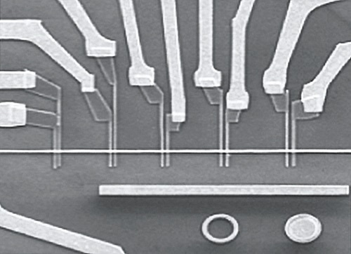
- Nanomanipulation, nanoprobing, nanoprofilometry
- Focused Electron Beam Induced Processes (FEBIP)
Column Technology
- Gemini
- Electron
- 30 kV
- Inlense SE detector
- Energy selective BSE (EsB) detector option
Stage
- 4” full travel
- Large Z travel
- Rotation and tilt option
Unique Writing Mode
Gemini-type e-beam column for broadest nanoengineering application bandwidth. Image credit: Raith
Nanoengineering, Nanomanipulation and Focused Electron Beam Induced Processes (FEBIP)
- Wide range of nanofabrication processes
- Improved TFE electron column offering the smallest beam size in the world
- Upgradable and open platform concept
- Unique stitch-error-free writing modes, traxx and periodixx
- Multiple detector concepts for unparalleled flexibility in mark recognition, analytical and imaging applications
- Raith NanoSuite: Full software interface with all modules totally integrated
Expandable Research Tool Concept
eLINE Plus´s modularly expandable research tool concept allow users to upgrade and adapt their system to existing trends in nanoresearch even long after the system is purchased. The eLINE Plus, by spanning beyond the “classical EBL application range”, makes way for interdisciplinary activities – across several fields of research.
The smallest electron beam size of 1.6 nm, prodived by an EBL system, indicates an indisputable prerequisite for analyzing the maximum resolution nanofabrication beyond boundaries – whether in nanolithography or other focused electron beam induced processes (FEBIP).
TwinLITH – Combining the Strengths of EBL and FIB
The perfect solution for next-generation nanofabrication is offered when a Raith electron beam lithography tool is integrated with a Raith focused ion beam system. Since the Raith systems share a software and hardware platform, it is possible to realize perfect synergy of 2D EBL resist accelerated lithography and 3D direct FIB patterning. The shared lithography architecture allows easy exchange of GDSII designs, job lists and sample holders, and thus permits efficient and advanced nanofabrication.
These two separate and complementary systems permit the working of additional nanofabrication tasks in parallel without losing time or compromising the whole benefit of either nanofabrication method. It is possible to write with two hands in a simultaneous manner and make the most of every single tool’s strengths for patterning, process development and control.
eLINE Plus Nanolithography Applications
Sub 5 nm lines in HSQ e-beam resist (Image Credits: J. Yang, D. Morecroft, M. Mondol, K. Berggren, MIT, and J. Klingfus, Raith USA)
Metallic lateral spin valves (Image Credits: F. Casanova et al., CIC nanoGUNE, San Sebastian, Spain)
Dense devices: 1 kB crosspoint RRAM (Image Credits: Sunghyun Jo, University of Michigan, USA)

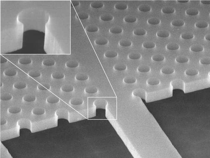
Advanced EBL: Photonic crystal structure in membrane (underetched) (Image Credits: William Whelan-Curtin, University of St. Andrews, UK)
Exact neurite guidance by nanogratings (Image Credits: Laboratorio NEST Pisa, Nano Lett. 2011, 11, 505-511)
eLINE Plus Nanoengineering Applications
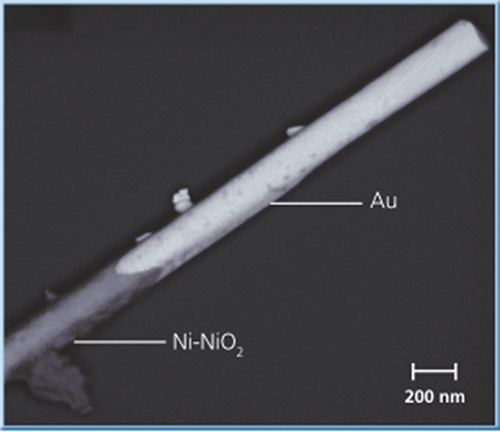
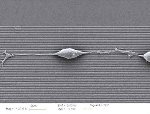
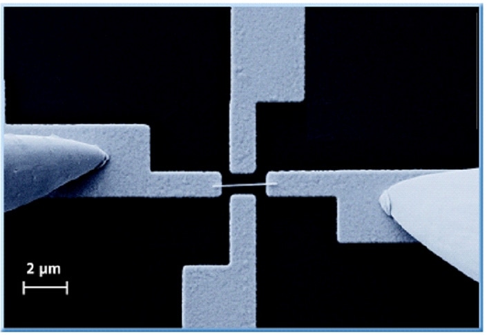
Nanoprobing of freely suspended Pt-nanowire, deposited on gold contact pads with EBID
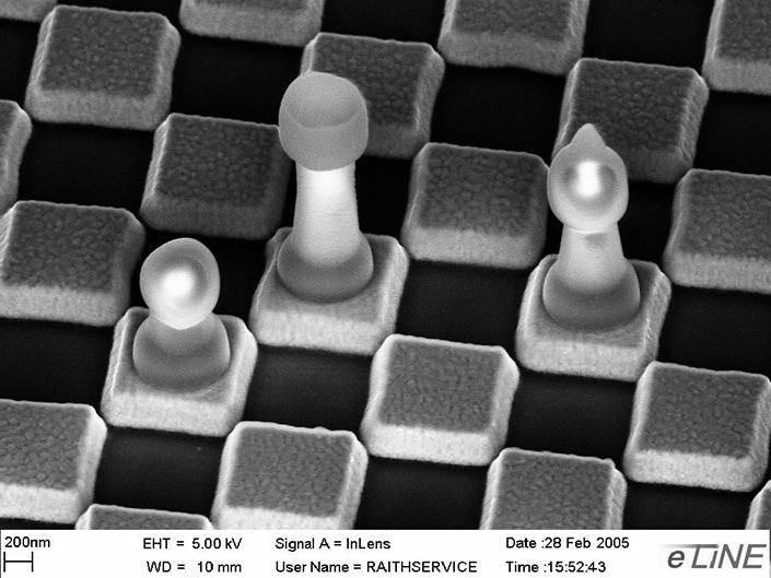
3D nanosculpturing by electron beam induced deposition (EBID)
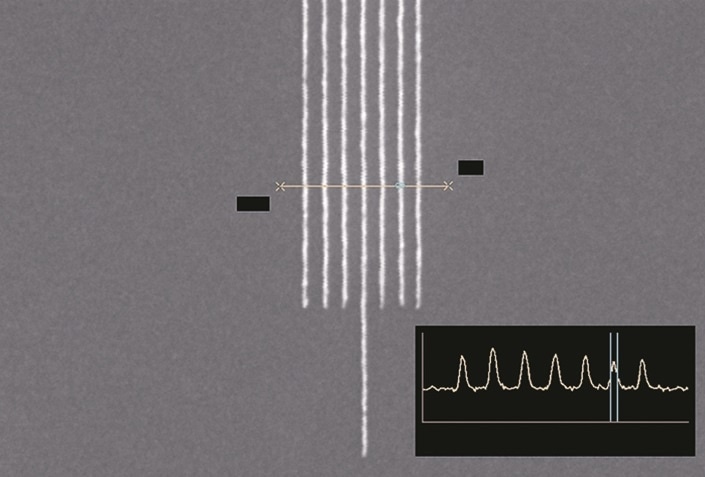
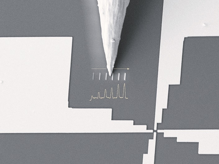
EBID-Deposit nanoprofilometry for growth rate determination (Raith)
Material contrast with energy selective inlens BSE-detector