PlasmaPro ASP has been developed to guarantee high-quality materials that can be deposited quickly and with the flexibility to run numerous chemistries to produce outstanding layers for integration into devices. It is based on a production-proven platform for corporate/specialized R&D. For increased throughput and thicker films, the state-of-the-art plasma-enhanced ALD system provides flexibility, conformality, and tunability at a fast pace.
- Enhanced serviceability and maintenance
- Low volume chamber for speed
- Low substrate damage
- Higher process stability
- Three times faster than conventional remote plasma
- Lower precursor consumption, which lowers operating costs and is environmentally friendly
- High material quality
- Low cost of ownership
PlasmaPro ASP has shared platform with Atomfab to provide quick and low-damage remote plasma-enhanced ALD. In comparison to thermal ALD and direct plasma ALD, remote plasma ALD provides higher device performance. It is small to reduce the effective chamber capacity for quick gas exchange and works throughout the whole 200 mm wafer diameter.
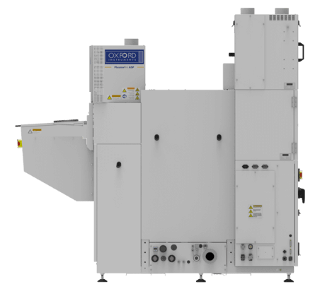
Image Credit: Oxford Instruments Plasma Technology
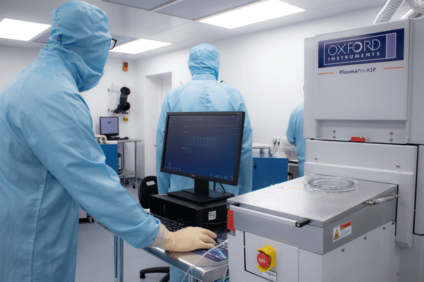
Image Credit: Oxford Instruments Plasma Technology
Features
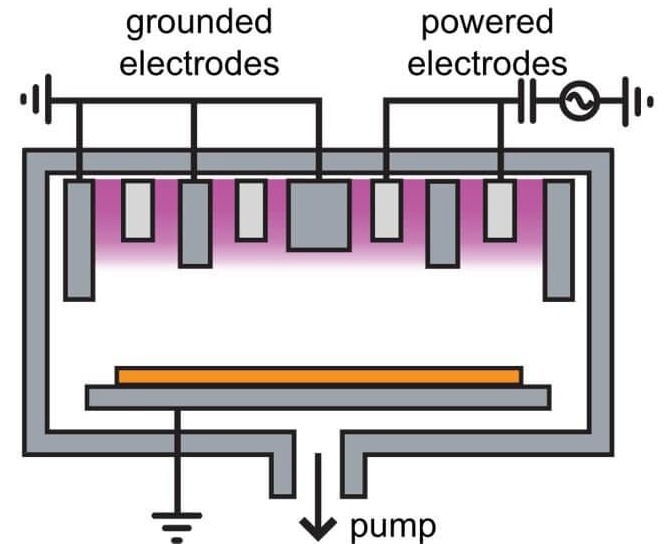
Image Credit: Oxford Instruments Plasma Technology
- High-speed remote plasma source
- High and homogeneous radical density and low ion energies for reduced damage and rapid saturation
- PLC and AMU control enables quick striking
- Excellent precursor and process control
- Up to 6 precursors, bubbled or vapor drawn
- Wafer electrode
- 200 mm wafer electrode with bias
- Up to 400 °C deposition temperature
- 200 °C heated inner chamber
- Control system
- Simplified wiring and ease of service
- Enhanced diagnostics for service
- No distinct 'electronics' rack
Applications
- Low damage GaN HEMT passivation for power electronics and radio frequency devices
- Low damage graphene encapsulation for Datacom applications
- Low-oxygen content conductive nitrides with all-metal plasma source facilitating rapid cycle durations, ideal for quantum devices
130 nm conformal superconducting NbN deposited in 8:1 aspect ratio trench using PlasmaPro ASP. Image Credit: Oxford Instruments Plasma Technology
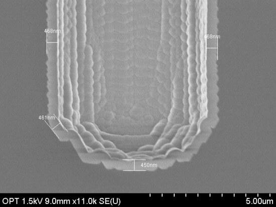
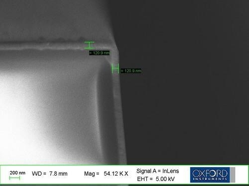
450 nm conformal SiO2 deposited in 32:1 aspect ratio trench using PlasmaPro ASP. Image Credit: Oxford Instruments Plasma Technology
Specifications
Source: Oxford Instruments Plasma Technology
| Specifications |
PlasmaPro ASP |
| Precursor Lines |
Maximum 6 (any combination) |
| Precursor size (ml) |
200 |
| Precursor type |
- Vapour draw - cooled
- Vapour draw - heated
- Bubbled – heated
|
| Handling |
Loadlock |
| Gas pod |
4 Process + 1 Ar (Onboard) |
| Electrode |
400 °C grounded/ biased |
| Roughing Pump |
600 m3/hr |
| Compliance |
UL Standard, Designed for SEM 2S |
| Software |
PTIQ |
| PEALD Process Library |
Al2O3, SiO2, NbN, TiN, more in development |