Researchers from Empa and the Maz Planck Institute for Polymer Research have successfully created a new way to selectively dope graphene molecules with nitrogen atoms.
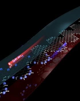
 This is an illustration of a p-n junction in a heterostructure made of pristine and nitrogen-doped ("glowing blue") graphene nanoribbon segments.The steep change in electrostatic potential across the interface region is expected to lead to high charge carrier separation efficiency, as schematically illustrated by oppositely moving electrons (red) and holes (blue).
In this method, “heterojunctions” were created in the nanoribbons by sequencing together the doped and undoped graphene segments, therefore fulfilling the first key step towards building a transistor.
These nanoribbons were grown on the gold substrate and later transferred onto a material that is non-conducting in nature.
When normal pieces are stringed together with nitrogen-doped pieces on a gold surface, heterojunctions are produced between the separate pieces. These heterojunctions exhibit similar properties as the standard p-n-junction. When a voltage is applied, the structure enables electrons and hole pairs to be easily separated. The study was published in Nature Nanotechnology.
Furthermore, the researchers have solved a major issue for integrating graphene technology to the semiconductor sector.
It is important to understand that graphene nanoribbons on a metal substrate, in this case gold, make it impossible for use as electronic switches. Gold or any other metal will cause a short circuit and disrupt the semiconductor properties of the nanoribbon.
Researchers have now shown that using a considerably easy etching and cleaning technique, the effective transfer of graphene nanoribbons is possible onto any substrate such as silicon oxide, calcium fluoride or sapphire.
Another paper published in Nature Communications also from Empa described the application of graphene strips in photovoltaics. They have noted that graphene nanoribbons absorb light in an exceptional manner and hence can be used as the absorber layer in solar cells. They also suggested that unlike graphene, light absorption can be regulated in a controlled manner.
References