Mar 6 2017
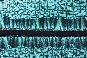
 Crystallization behavior can be controlled locally, creating regions with different crystal patterns. Credit: � 2017 KAUST
Customized polycrystals that can be used for fabricating highly versatile and faster semiconductors have been developed, due to an accidental observation of crystals that formed a mark similar to the stain left by a coffee cup on a table.
A wide range of electronic and optoelectronic devices are developed using thin-film semiconductors as their base materials. Such devices are typically fabricated through crystallization techniques that produce polycrystals including a disorderly mixture of individual crystals having disparate sizes and orientations.
A research team headed by Material Science and Engineering Professor Aram Amassian from King Abdullah University of Science and Technology (KAUST) has achieved significant development in the control of crystallization.
The team included researchers from the KAUST Solar Center as well as researchers from the University’s Physical Science and Engineering Division in partnership with Cornell University.
There is no longer a need to settle for random and incoherent crystallization.
Aram Amassian, Professor, KAUST
The recent findings of the research team began when Dr Liyang Yu from the KAUST group observed that an outer coffee-ring shape was formed when a droplet of liquid semiconductor material dried, where the coffee-ring shape was extremely thicker when compared to material at the center. When Yu initiated crystallization of the material, it was the outer ring that crystallized first.
“This hinted that local thickness matters for initiating crystallization,” stated Amassian, where the finding was in contrast to the existing knowledge on the formation of polycrystal films.
The anomaly inspired the research team to pursue a detailed analysis in this area. The researchers discovered that they can use the thickness of the crystallizing film to influence the crystallization process of various materials. Most importantly, when the thickness was tinkered, the orientation and position of the crystals could be minutely controlled in various regions in a semiconductor.
We discovered how to achieve excellent semiconductor properties everywhere in a polycrystal film.
Aram Amassian, Professor, KAUST
Amassian further added that by seeding various patterns of crystallization at varied locations, the researchers were able to develop bespoke arrays that can be used in electronic circuits.
Such a process comes as a major advancement to the traditional practice of using materials whose optimum characteristics are not sustained through the whole polycrystal nor whose functions at varied regions can be controlled.
“We can now make customized polycrystals on demand,” stated Amassian.
Amassian anticipates that this breakthrough would culminate in the development of customized, high-quality polycrystal semiconductors, thus enabling advances in photovoltaics, optoelectronics, and printed electronic components.
The new technique can potentially lead to innovative solar power generating systems, highly efficient consumer electronic devices (with lightweight and flexible parts), and improvements in medical electronics. All of this has been possible by the accidental observation of the odd pattern in a semiconductor droplet.
In the near future, the research team will work toward taking their research from the lab to real life through research collaborations and industry partnerships.
The coffee-ring effect leads to crystallization control (1:1)