In the recent study published in the journal Molecules, researchers studied the characterization and growth of graphene on different types of copper (Cu) surfaces.
Study: Growth and Characterization of Graphene Layers on Different Kinds of Copper Surfaces. Image Credit: ktsdesign/Shutterstock.com
Graphene and Optoelectronic Devices
Graphene is a promising material for developing novel optoelectronic devices due to properties such as high ballistic transport and carrier mobility with more than 97% transparency for visible light. Studies have demonstrated that chemical vapor deposition (CVD) is the most effective method to grow graphene for optoelectronic applications.
The advantage of using CVD is that it produces high-quality and low structural defect density graphene, which is critical for industrial and research applications. Moreover, CVD technology also provides chemical inertness and impermeability to most gases, making it highly effective for growing graphene intended for anti-corrosive coating materials. The fundamental limitation of CVD is the inability to achieve non-defective graphene growth over sufficiently large areas.
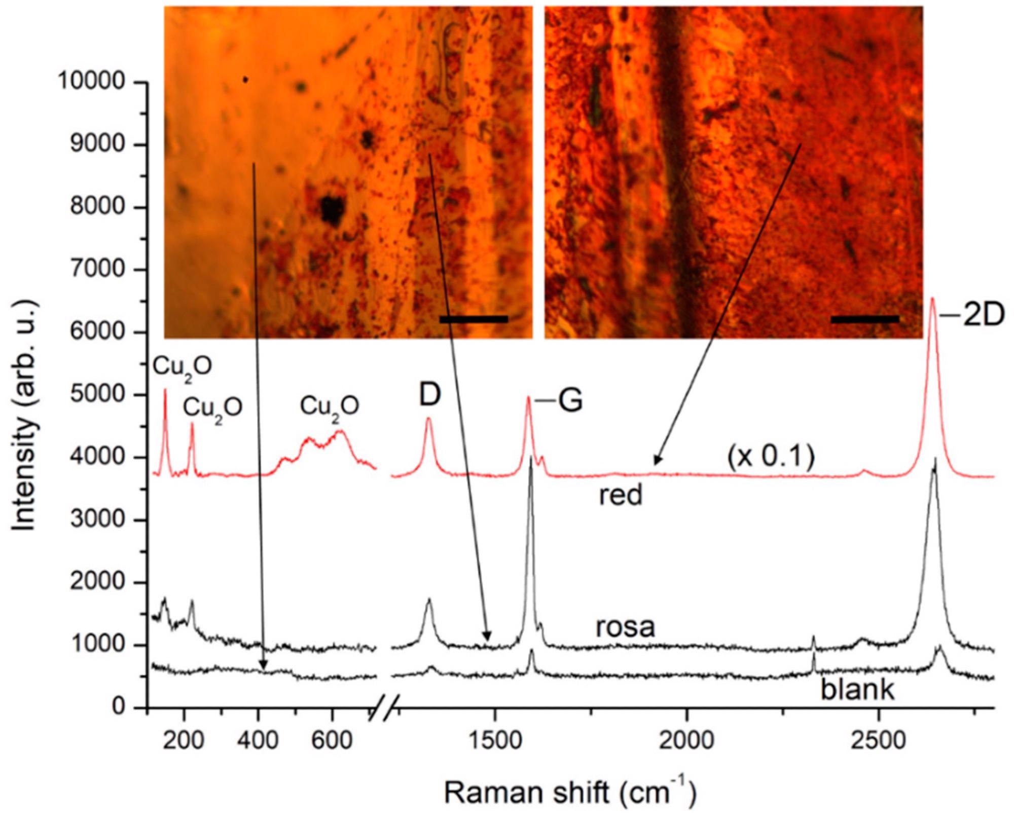
Micro-Raman spectra from different regions of a Gr/Cu foil several months after the CVD graphene growth process. The traces are plotted after background subtraction for clarity. Insets: microscopic images from the corresponding regions with exact specification of the spots of laser excitation. The scale bars represent 100 μm. Image Credit: Rafailov, P.M et al., Molecules
In the present study, the CVD method was used to grow graphene on different kinds of Cu surfaces. The primary motivation of the researchers was to find the most suitable Cu surface to get defect-free graphene for optoelectronic devices.
Methodology
The researchers used both raw and electropolished Cu foil for growing substrate. During which, the electropolishing was conducted, keeping polished Cu foil as an anode, and a Cu plate as the cathode. Additionally, the process was performed at room temperature using a specific polarization voltage and using concentrated H3PO4 solution as an electrolyte.
In the next step, the anodic dissolution in a mass-controlled kinetic regime was conducted for 15 min, followed by rinsing the samples in deionized water. Finally, the specimens were transferred to the growth chamber, and electropolishing was evaluated by visual inspection and gloss and optical microscopy. It must be noted that the samples were compared with the surface to an untreated foil during the visual and microscopic examination.
The graphene was grown using low-pressure CVD (LPCVD). The researchers used LPCVD for graphene growth because it produces lower graphene nucleation density, and catalyst surface reactions control the graphene growth rate during the process. Cu foil was annealed in an argon/hydrogen atmosphere during the process, and CH4 with H2 flow was introduced in the reaction chamber intended for the growth stage. Further, the sample was cooled in a hydrogen/argon atmosphere, and the grown samples were maintained in a clean environment before experimentation.
The obtained samples were characterized by Raman spectroscopy, electron backscatter diffraction, and X-ray photoelectron spectroscopy. The characterized was performed at three different sample storage times: fresh, six months, and 20 months. Additionally, the researchers also analyzed the effect of electropolishing on the metal surface.
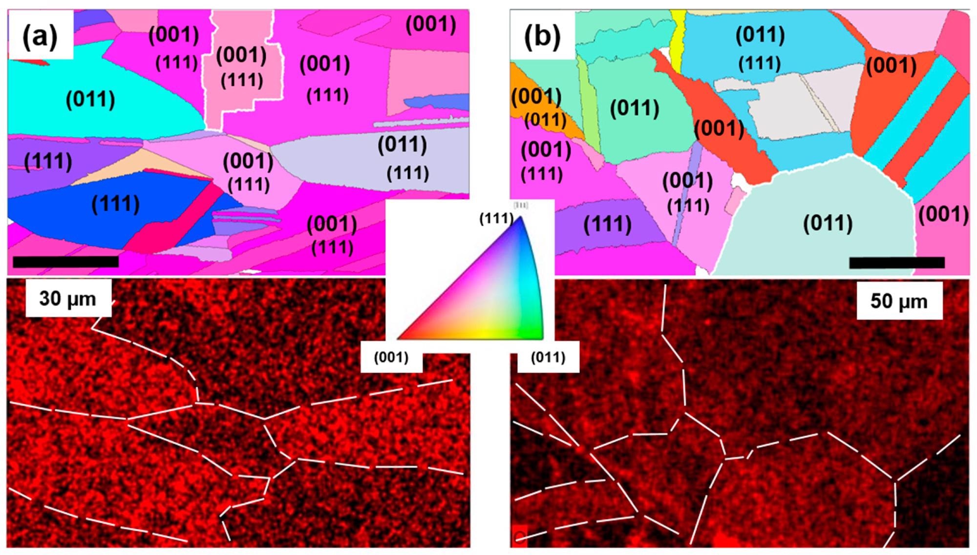
(a) EBSD orientation map of the investigated spot on the “fresh” sample (top) with corresponding EDX oxygen elemental distribution map (bottom). (b) Same as (a) for sample “6 months”. In the top panels, for grains with incomplete low-index orientation, the minor component is indicated in smaller font below the dominant one. Bottom panels: some Cu grains are delineated by a dashed line for clarity; the intensity of the red coloring corresponds to the oxygen concentration. Inset: orientation color code. Image Credit: Rafailov, P.M et al., Molecules
Results
The time evolution study of graphene-coated Cu revealed that the graphene-Cu foil has regions with different color contrasts after extended storage at ambient conditions. The difference in color contrast represented the different oxidation degrees in which yellow, pale-red, and red colors indicated blank copper, slight oxidation, and heavy oxidation, respectively. The results also indicated Cu-graphene solid coupling on the non-oxidized Cu grains.
The electron backscatter diffraction and energy dispersive X-ray analysis results for the fresh samples and the sample kept for six months shows that most grains were not perfectly oriented according to the primary Miller indices. Further, the depicted orientation maps revealed that dominantly (011) oriented Cu grains were the most susceptible to Cu2O formation in both graphene-coated samples, and the grains with dominant (001) orientation had the lowest oxidation. Due to this, the Cu-graphene solid coupling and strain in the graphene lattice are released in a time-scaled and non-uniform manner.
The ellipsometric results demonstrated the presence of an oxide layer beneath the graphene, which ranges from 6–7 nm. It must be noted that the range of the fractional parts was calculated based on previously published studies.
The visualization of graphene grains using liquid crystal coating indicated that the graphene grown on electropolished Cu foil has larger grains with lower defect density. The lower defect in the graphene grain is significant for the high performance of the optoelectronic devices developed through it. Additionally, the presence of large grains is significant for reduced oxidation in graphene-coated metals.
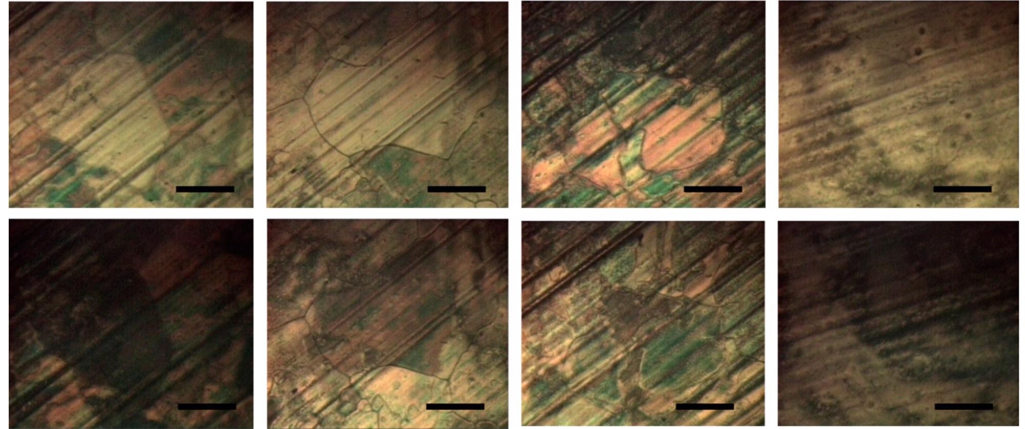
Four vertical pairs of microphotographs of E7-coated graphene (top—bright state; bottom—dark state achieved after rotation at 45°). The images depict: graphene grains on electropolished Cu foil (left two pairs) and on nonprocessed Cu foil (right two pairs). The scale bars represent 100 μm. Image Credit: Rafailov, P.M et al., Molecules
Conclusions
To summarize, the researchers showed that defect-free graphene could be grown on a large Cu surface with the process used in this study. They discussed the time-dependent changes, calculated the thickness of emerging Cu2O beneath the graphene, and examined the orientation-dependent affinity to oxidation of different Cu grains. Future studies must estimate the number of graphene layers required to produce optimized results.
Source
Rafailov, P.M.; Sveshtarov, P.K.; Mehandzhiev, V.B.; Avramova, I.; Terziyska, P.; Petrov, M.; Katranchev, B.; Naradikian, H.; Boyadjiev, S.I.; Cserháti, C.; et al. Growth and Characterization of Graphene Layers on Different Kinds of Copper Surfaces. Molecules 2022, 27, 1789. https://www.mdpi.com/1420-3049/27/6/1789
Disclaimer: The views expressed here are those of the author expressed in their private capacity and do not necessarily represent the views of AZoM.com Limited T/A AZoNetwork the owner and operator of this website. This disclaimer forms part of the Terms and conditions of use of this website.