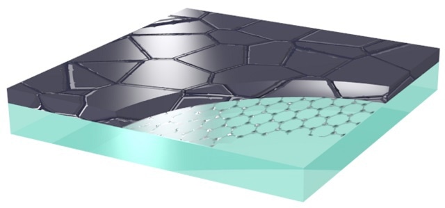
Graphene moves a step closer to real-world applications in solar cells. Image credit: photos.com
New research has shown that graphene maintains its beneficial properties when coated with silicon, marking another step towards the use of the ‘wondermaterial’ in photovoltaic arrays.
Graphene has long been thought of as a potential candidate for use in solar cells, due to its high conductivity, transparency and relatively economical price tag. It is thought that graphene could be used to produce transparent contact layers in solar panels for the conduction of electricity, without reducing the sunlight received by the panel.
However, questions have been raised about the application of graphene in commercial solar cells, because the interaction of graphene with adjacent materials can alter its properties substantially.
Now research at the Helmholtz-Zentrum research centre, Berlin, has shown that the properties of graphene actually change very little when it is coated with both amorphous and poly-crystalline silicon, two variations that are often used in silicon thin-film technology.
Furthermore, the team found that from testing the mobility of the charge carriers within the graphene that the layer of 2D carbon demonstrates charge carrier mobility 30 times greater than that of zinc oxide, a common material currently used for solar contact layers.

Graphene was deposited onto a glass substrate. The ultrathin layer is but one atomic layer thick (0.3 Angström, or 0.03 nanometers), although charge carriers are able to move about freely within this layer. This property is retained even if the graphene layer is covered with amorphous or polycrystalline silicon. Credit: Marc A. Gluba/HZB
One of the co-authors of a paper outlining these findings, Norbert Nickel, summarises below the surprise and delight of the research team.
"That's something we didn't expect to find, but our results demonstrate that graphene remains graphene even if it is coated with silicon."
The process involved in this discovery was not a simple procedure to undertake, and involved growing the graphene on a thin copper sheet, before transferring it to a glass substrate so that it could be coated with thin-film silicon.
Another co-author, Marc Gluba, explains some of the difficulties encountered when conducting such delicate research.
"Admittedly, it's been a real challenge connecting this thin contact layer, which is but one atomic layer thick, to external contacts. We're still having to work on that."
Though the research was conducted on a sample only one square centimetre in size, it is hoped that the technique can be applied to panels of a much larger surface area.
This new research is yet another recent example of researchers making great strides towards the commercialisation of graphene, solving problems that have previously rendered the material’s use untenable in real-world applications.
For example, Michigan Technological University recently conducted research that showed how a 3D version of graphene could become a viable replacement for expensive platinum in dye-sensitized solar cells.
And just last month, both MIT and the Vienna University of Technology published work describing how graphene light detectors could be combined with semiconductor chips for computing applications.
Original source: Helmholtz-Zentrum Berlin für Materialien und Energie
Disclaimer: The views expressed here are those of the interviewee and do not necessarily represent the views of AZoM.com Limited (T/A) AZoNetwork, the owner and operator of this website. This disclaimer forms part of the Terms and Conditions of use of this website.