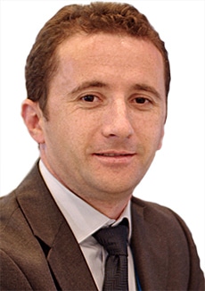
Dr. Daniel Goran, product manager at Bruker Nano GmbH, speaks to AZoM about the benefits of using Transmission Kikuchi Diffraction (TKD) for nanomaterial characterization.
What industry does Bruker Nano Analytical work within?
The Bruker Nano Analytics (BNA) Division, headquartered at Bruker Nano GmbH in Berlin, Germany, develops, manufactures and markets X-ray systems and components for elemental and structural analysis on the micro- and nano-scale. The product range includes analyzers for electron microscopy as well as X-ray fluorescence spectrometers.

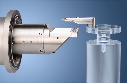
Bruker's TKD Detector Head - the OPTIMUS™
What is Transmission Kikuchi Diffraction (TKD)?
The Transmission Kikuchi Diffraction (TKD) technique, a.k.a. transmission EBSD (t-EBSD), has been recently introduced as a Scanning Electron Microscope (SEM) based method capable of delivering the same type of results as EBSD, but with up to 10x better spatial resolution.
After its introduction a few years ago, TKD was quickly adopted by the scientific community as it fills the spatial resolution gap between EBSD and electron diffraction techniques in a Transmission Electron Microscope (TEM), i.e. from 100 nm down to a few nm.
How does this differ from Electron Back Scatter Diffraction (EBSD)?
The TKD technique uses a signal (Kikuchi patterns) captured from underneath an electron transparent sample, while the EBSD signal is produced by back scattering diffracted electrons escaping a highly tilted bulk sample. The two techniques are also referred to as “transmission mode” and “reflection mode” respectively.
When would you use TKD over EBSD?
TKD technique’s spatial resolution performance makes it the best choice for quantitative characterization of nanomaterials or ultrafine grained materials with crystal/particle sizes from 10 to 100 nm. In certain cases, characterization of deformed or heavily deformed structures would also benefit from the smaller interaction volume of the TKD technique.
Additionally, there is currently an increasing interest in using TKD in SEM for residual strain analysis due to the sharper resolution found in TKD patterns as compared to standard EBSD patterns.
What are the main difficulties with carrying out TKD with an EBSD detector head?
Current EBSD detectors were not designed to work in TKD mode and therefore the sample / detector geometry is not optimum. To be more specific, when using a standard EBSD detector for TKD analysis the signal will not be acquired from where is strongest and the Kikuchi patterns will display strong distortions that will affect the subsequent analysis.
What are the key advantages of the OPTIMUS™ TKD detector head?
The OPTIMUS™ TKD detector head was developed to solve the two main TKD issueswhen using a standard EBSD detector as detailed above. The unique design allows the user to place it underneath the electron transparent sample, thus acquiring the Kikuchi signal where it is strongest and with minimal gnomonic projection induced distortions.
Experimental results have shown that the OPTIMUS™ TKD detector head provides a signal increase by at least a factor of twelve.
This means that orientation mapping in transmission mode is now faster, with an improved spatial resolution and with better data quality, or indexing rate. OPTIMUS™ has been additionally fitted with the already famous ARGUS™ imaging system to provide dark field / bright field imaging capabilities. OPTIMUS™ TKD practically transforms an SEM into a low kV TEM.
What other equipment is required to use with the OPTIMUS™ detector head?
OPTIMUS™ is an add-on hardware option for all e-Flash EBSD detectors and, of course, it additionally requires the ESPRIT software for analysing the patterns. We also recommend using the Bruker designed TKD sample holders but this is not a must.
How easy is it to switch between the different analysis setups?
The standard EBSD detector head can be exchanged with OPTIMUS™ and vice-versa by a trained user in less than 20 minutes. To simplify the exchange procedure both OPTIMUS™ and the standard EBSD detector head have been designed with “plug&play” capabilities. The phosphor screens on both detector heads and ARGUS™ diodes are user replaceable as well.
TKD is a relatively new technique – how do you expect SEM techniques to further develop in the near future?
The “birth” of TKD, and its fast adoption by the research community, is a direct result of the analytical needs brought by the technological changes we’ve been experiencing recently.
In addition to new or improved capabilities for characterizing nano-materials, I expect that in the near future, we will see a significant effort in the development of analytical capabilities for characterizing functional materials. These are two of the most important materials science fields that are driving the technological advancement we experience today.
How will Bruker be involved in these developments?
Our product development strategy is defined by our close collaboration with top research groups in the EBSD field. OPTIMUS™ is just one example of such collaboration and is an answer to the current analytical needs of the scientific community.
We are also investing a lot of effort in pushing the limits of what the EBSD technique could be used for when analysing “exotic” phases in functional materials. The QUANTAX EBSD has a very powerful “Phase ID” feature, and the unique capability of calculating pattern simulations using the dynamical theory of electron diffraction.
Using dynamical simulations and image correlation, we are confident that in the near future, the EBSD technique will be able to take advantage of the full richness of information provided by a Kikuchi pattern, and will be used for advanced applications like lattice parameter refinement or absolute elastic strain measurements.

About Daniel Goran
In 2002, Daniel graduated as a metallurgical engineer from Polytechnic University in Bucharest, Romania and, one year later, got his M.Sc. degree from Louis Pasteur University in Strasbourg, France.
In 2007, Daniel received his Ph.D. from Lorraine University in Metz, France on the heterogeneity of severe plastic deformation.
After a short experimental PostDoc, he moved to Hobro, Denmark where he started working for Oxford Instruments HKL as EBSD Application Scientist.
In June 2009, he moved to Berlin, Germany to join Bruker Nano’s EBSD team as application scientist. Since July 2012, he has been responsible for the EBSD system as Product Manager.
Disclaimer: The views expressed here are those of the interviewee and do not necessarily represent the views of AZoM.com Limited (T/A) AZoNetwork, the owner and operator of this website. This disclaimer forms part of the Terms and Conditions of use of this website.