In order to enhance the performance and reliability of microstructures, it is essential to have an accurate knowledge of their mechanical properties. Nanoindentation provides a standardized approach for measuring the geometry independent material properties of small structures or thin films. Together with an accurate measurement of the microstructure’s geometry, the overall mechanical behavior can be measured.
A alternative method can be used where the mechanical behavior of the microstructure can be directly calculated on the structure itself. However, because of the extensive range of varied structures types, shapes, and sizes, this demands a highly versatile instrument that fits the requirements of all of these diverse structures.
In addition, microstructures often have a dynamic role to play, for example in coatings, actuators, or sensors. Examples for such active microstructures include dry adhesives, super-hydrophobic surfaces, electro-active polymer actuators or micro-capsules. In order to have a quantitative understanding of these active microstructures, their behavior cannot be modeled accurately and should be quantified on microstructure level.
The most versatile micromechanical testing system, FT-MTA03 Micromechanical Testing and Assembly System, enables a complete analysis of the mechanical properties of microstructures. This article outlines a range of the testing principles and applications.
Nanoindentation for the Qualification of Young’s Modulus of Micromaterial
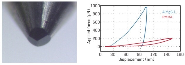
The FT-MTA03 provides both force-controlled and position-controlled nanoindentation, and can be used for the localized material testing of small volumes. During the load application, the tiltable microscope enables visual observation of the sample in real time.
Nanoindentation into Soft Materials
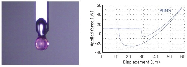
The FT-MTA03’s wide displacement range coupled with the low-force sensing capabilities makes it a perfect tool for soft material characterization. In the experiment, the PDMS sample is indented with a spherical tip. In addition to the standard material parameters, the raw force-displacement-time data is supplied for different material models.
Mechanical Property Mapping of a Suspended Diamond Membrane
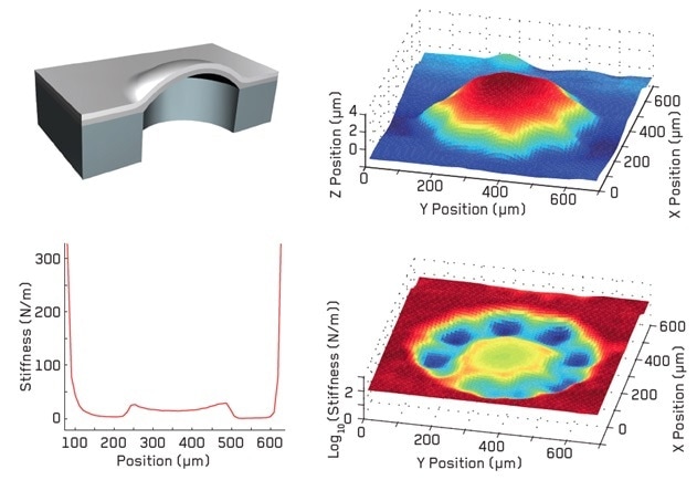
The testing of a nanocrystalline diamond and aluminum nitride membrane for use in tunable micro-optics is described here. The membrane’s stiffness and topography are calculated. The topography of the micromembrane is illustrated in the upper right graph, while its stiffness distribution is shown in the lower right graph. The lower left graph is a cross-section of the stiffness map passing via the central section of the membrane.
Dimensional Metrology of Microstructures
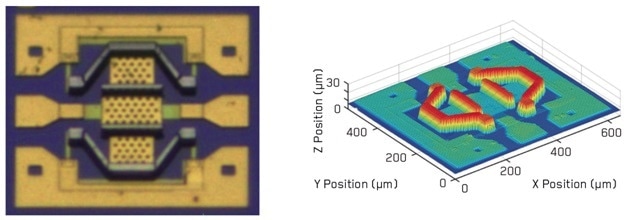
Advancements in microtechnology enable the fabrication of extremely smaller, high aspect ratio structures. This miniaturization leads to increased mechanical and dimensional deformations. The FT-MTA03 is capable of measuring the mechanical properties and dimensions of the microstructure for the optimization of fabrication processes. (Device courtesy: Prof. Ionescu, Nanolab, EPFL)
Micromechanical Testing Along Different Directions
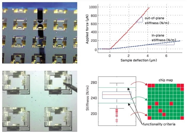
During the micro-manufacturing process development, a large amount of process parameters influence the mechanical properties of the MEMS structures. In this application, both the out-of-plane stiffness and in-plane stiffness of a range of MEMS flexures are examined using the FT-MTA03 Micromechanical Testing and Assembly System.
By defining a lower and an upper limit for the target stiffness, a chip map is generated to detect the working flexures (green) and flexures that are beyond the required specifications (red). Flexures with cracks (low stiffness) or flexures that have not been properly discharged from the wafer (very high stiffness) are identified. It is simple to compute the yield rate by the ratio of green to the total number of devices.
Electro-Mechanical Behavior of Active Materials
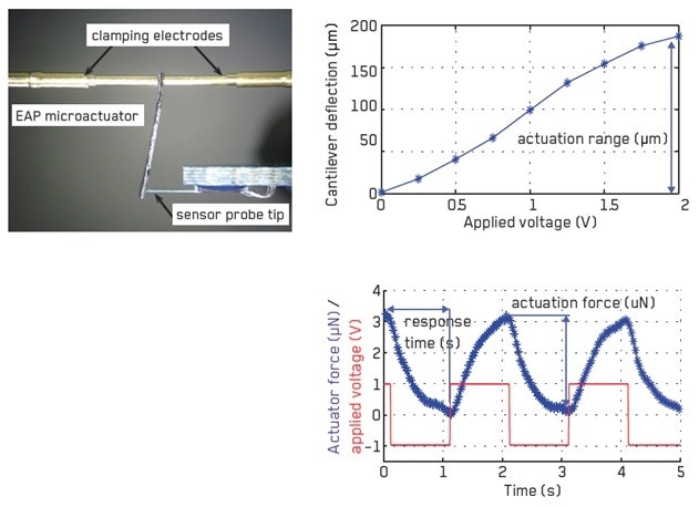
Conducting or conjugated polymers are receiving a great deal attention as smart materials for innovative microfabricated devices, including sensors and actuators. In this application, the actuation force, the deflection range, and the time-response of the beam-shaped electroactive polymer (EAP) actuator are tested.
When the beam-shaped microactuators are clamped between two electrodes, it enables the actuation signal to be applied to drive the microactuator. The maximum deflection of the EAP actuator beam tip versus the actuation voltage is shown in the top graph. The lower graph displays the driving force produced by the EAP actuator and the square-wave driving signal plotted against time.

This information has been sourced, reviewed and adapted from materials provided by FemtoTools AG.
For more information on this source, please visit FemtoTools AG.