In this interview, Scott Jordan, Head of Photonics at PI (Physik Instrumente) talks to AZoM about the importance of manufacturing and testing photonic devices.
What is photonics and why is it important?
First, let’s consider electronics. It is a very important field because everything we do today is based on electronics. Photonics is based on the same principle, but it uses photons instead of electrons. There are benefits in terms of speed, capacity, energy, and efficiency; plus, there are new things like quantum computing and quantum communications that have a significant photonic element to them. This is going to change everything, and that is why photonics is important.
Technology is changing every day in the world. Why is it important to know more about these changes than ever before?
It is important to know about these changes because they are going to impact our lives in deeper and broader ways than ever before. We have so many demands for data today. For example, look at the pandemic that the entire world is confronting today. Every day you read about efforts to develop therapies, vaccines, treatments, etcetera.
You can imagine how important fast communications are to the medical world just to ensure that all the doctors and medical researchers in the world can be aware of, and build upon, each other's work.
Then there are areas such as genomics. The virus is being sequenced, a process that uses photons to determine the arrangement of the genes in the virus, which is incredibly important to know in order to answer questions such as: Does it mutate? How rapidly if so? In what ways does it mutate? This is fundamental to understanding the life cycle and biology of the virus and how it infects human cells. And this generates lots of data, which must be stored and communicated and correlated.
It is also important to understand whether a potential vaccine can work. Will there be immunity? If someone has been exposed to the virus before, or they have battled it and survived the infection, could they face this again if the virus mutates even slightly? These are all questions that are being answered, with photonics playing a fundamental role.
Furthermore, there is the personalized medicine field that has been part of our medical lives for some years now. Let me give an example. If you were to go to your doctor with a tumor and the doctor wants to know what they are dealing with, they will take a biopsy of that tumor and perform a genetic study on it. This study correlates it against thousands of other cases so that they can select which therapy has worked best in other situations, based on facts.
Another example is seen in communications, especially in video calling on platforms such as Zoom, Skype, and Webex, which are all internet-based technologies. The internet today is increasingly photonics-based because photonic networking offers more capacity and efficiency than electrons. It is higher throughput, more expandable, and more scalable.
Consider Zoom. Since this pandemic started, the demand for Zoom's services for performing web conferences and telepresence has increased by a factor of 20 in just the first month. Now imagine you are trying to run a business and need to accommodate that kind of growth in such a short amount of time. In one respect, it is a good problem to have because it means that you are doing things right and providing a service people want. But on the other hand, it is a big challenge to scale services so rapidly. Photonics makes that possible.

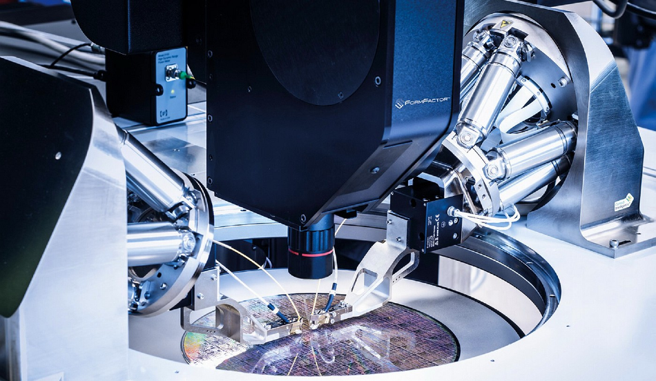
Silicon Photonics –the combination of electronics and photonics– in the future, combining significantly higher speed, data rates, and reduced power requirements. The downside is the higher complexity in manufacturing and testing. The image shows an 18-axis PI FMPA fast photonics alignment system mounted on a FormFactor Cascade Silicon Photonics wafer prober. Image Credit: FormFactor
What roadblocks and challenges are often faced when it comes to manufacturing and testing photonic devices?
If you wanted to connect to an electronic device, you might have contacts--for example on a semiconductor chip--that need to be connected to the outside world. The contacts might be 20 or 30 microns big. That is quite small, but it is something that you can do with a microscope and some simple positioners.
With a photonic device, when making a photonic connection, the contacts are about a hundred times more sensitive in terms of positioning. So with an electronic contact, you can be off by many microns and still be able to make good electronic contact. For a photonic device, your connection needs to be correct within perhaps 20 to 50 nanometers or so. This is very common and we see it a lot in our customers' applications today.
That right there is the biggest roadblock and the biggest challenge, getting that alignment absolutely correct so that photons can efficiently go from one device to the next device. Now, this alignment cannot be done using a microscope. You cannot see 20 nanometers with a microscope. It is optically not possible. So, that means that the actual coupling, the actual amount of light going from one device to the other, needs to be observed and optimized in real-time.
Traditionally, this has been a very slow process. I have spent my career working on this problem. Recently, we solved this problem in a very efficient way.
Think about if you have more than one photonic device, for instance, an array device that has multiple channels that need to be connected to other devices in the package and to the outside world. With this device, in addition to getting that transverse alignment correct to 20 or 50 nanometers, you also have to be correct in terms of angles so that all of the channels can line up. The problem is that you can do the alignment in X and Y in this transverse plane, but when you attempt to adjust the rotations to bring everything into the same plane, it is inevitable that it will damage the X and Y alignment as well.
The way people have traditionally dealt with this is by doing an XY alignment and making a small rotational alignment around the Z-axis to try to bring things into the same plane. But, because that causes problems in terms of X and Y, they have to stop, realign an X and Y, and then repeat that process over and over again. It can take several minutes.
Now imagine you have a wafer filled with silicon photonic devices. You need to test each of these devices on the wafer. Before you slice up the wafer and make individual chips, you need to know which of those chips actually work and are worth pursuing through the packaging process where the biggest costs are. That means you need to do this testing on the wafer of each device, which is called wafer probing.
There may be thousands of devices on that wafer that need to be tested. If it takes you several minutes to align each device, it can get very expensive. The speed of doing the alignment is really important.
The alignment is also very important for after the wafer stage as well. After you have tested the devices on the wafer, you need to package them, and the packaging might involve several dozen steps. During most of those steps, you need to repeat the whole process, perform new alignments for testing and for connecting things together. If it takes you several minutes to perform new alignments on the wafer, it is going to take you several minutes to do the same in each of the production steps, which can become very expensive.
How can PI help overcome these challenges?
What we have done is develop a unique technology that has won awards, because, in as little as one step, it can perform these alignments in multiple degrees of freedom, at multiple inputs and outputs, across multiple elements. Nobody else can do that.
It is about a hundred times faster than traditional methods. This directly improves the cost, the roadblocks, and the challenges of making photonic devices.

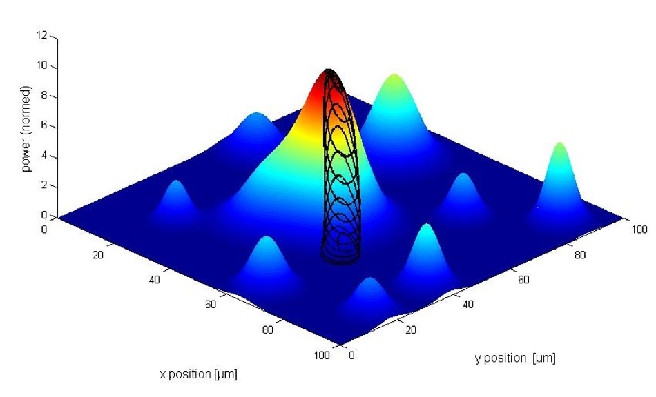
The fast digital gradient search algorithm finds the optimum signal in <1 sec.
How do the systems manufactured by PI compare to other vendors on the market? What sets them apart?
The most important difference is that our largest market has always been semiconductor manufacturing. You cannot make a chip of any sort today without PI components being present somewhere in the manufacturing chain. In the lithography column, PI positioners are used to manage the optical processes and to position things. At the other end of the production process, in the wire bonding in the final packaging of microchips, the PI mechanisms are used to form the little loops that connect the chip to the outside world. Similarly for the steps in between.

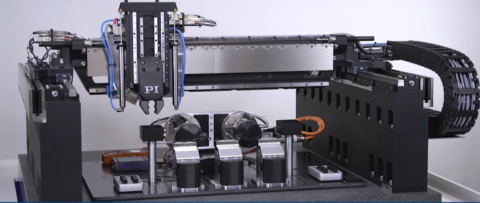
A system for automated photonics array alignment
We know how important speed, reliability, cleanliness, and performance are to semiconductor manufacturing and packaging. We have applied that knowledge to the photonic market as well because the whole field of silicon photonics is a result of the merger of photonics and the semiconductor industry. The semiconductor industry is what is driving this, and they are the ones that are suffering the costs of conventional alignment technologies.
What is different about us and what we can do to help concerns the speed, the throughput, the parallelism, and the ability to perform these alignments wherever they are required in the production process - from the wafer test, all the way up to final packaging, and at every step in between. We understand how to do that and we understand how important things like reliability, speed, throughput, and productivity are to the economics of manufacturing these devices. We know that because we have spent 50 years enabling the semiconductor industry.
Can you provide any examples or case studies of how photonic devices tested and manufactured using PI systems are being utilized in applications and industries?
We introduced this technology in 2016 and won a number of awards. Since then, we have established foundational technologies and foundational applications with our customers, who range from semiconductor manufacturers and foundries to tool makers. We have customers such as FormFactor and MPI who make wafer probers that incorporate this photonic alignment technology for very efficient testing of semiconductor chips.
At the other end of the spectrum, in the packaging arena, we have customers like Tegema in the Netherlands. They are currently manufacturing a ground-breaking packaging automation tool that is more compact and ten times faster than anything that has come before.
And keep in mind that many photonic device manufacturers set up their own custom machinery using in-house or partner integrators. We work with lots of those teams too.
What is in store for the future of photonics-related solutions developed by PI? Are there any new applications and industries that can benefit from them?
Yes, definitely. We have talked so far about silicon photonics, and there is still a lot of work that we are doing to broaden the applications and the availability of this technology for these customers. For example, last year we introduced the capability of doing these fast alignments on some very large stages that can accommodate big trays of components.
We have our hexapod micro-robots, that are very useful for performing multiple degrees of freedom and alignments. They are also very compact, with lots of capability including the full parallel alignment suite. We also have implemented these functionalities in our nano-positioning equipment, which is important because of the resolutions that are often required, and because nano-positioning mechanisms are really fast with no wear mechanisms, meaning that they practically last forever.
We now have a broader, more modular architecture than ever before in order to solve the specific problems that our customers bring to us.
We are finding more and more applications, too. This alignment process maps well to making cameras, objective lenses, and imaging systems of various sorts. There you may have lenses that need to be aligned in a time-consuming sequence that equates to cost.
Almost everyone carries a camera-equipped smartphone with them, and there are several billion smartphone cameras manufactured every year. With each better generation of cameras, the tolerances and the complexity of their optical design get more sophisticated, and that becomes a challenge in their manufacturing. We speed up that process using our technology.

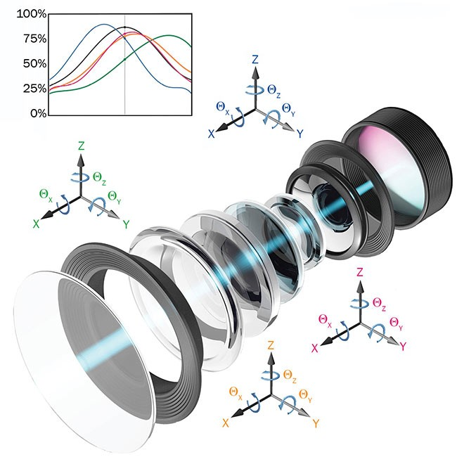
High-performance lenses, such as those found in cell phone cameras can consist of many individual optical elements that must all be aligned in multiple degrees of freedom
Lasers are another application. Building lasers is very complicated, as they have multiple elements that can be diffractive, refractive, reflective, and active, all of which need to be lined up. We are able to speed that process up, too. Our general-purpose optimization engine is now available across a comprehensive range of products and formats, and it is something we think can be a real cost-saver for broad new classes of manufacturing and testing.
Where can our readers go to find out more?
I hope that your readers can attend the webinars and remote seminars that we are providing during the pandemic. We are finding that that is a real productivity enhancer for our customers, for us to be able to visit on short notice without a lot of travel and risk of virus spread. These are all things that our customers value at this time.
In my home state, as we are all currently required to work from home, I have a complete demonstration set up with three cameras so that a customer can come to us and say, "Can you align this particular type of device?" or, "Can you perform this particular type of alignment or optimization?" and we can spin that up very, very quickly and be on their desk with the demonstration in a matter of minutes or hours.
This is something that is entirely new for our customers and for our marketplace, but it is actually very useful. I predict that it will be part of the new normal as the world begins to settle down and heal from this viral assault that we are all suffering from right now. And it's enabled by photonics!
Readers can go to the PI website, call their local PI office since we have engineers, applications specialists, and resources all around the world. We will make sure that we can answer customer questions and help them to be more productive in their particular application.
Disclaimer: The views expressed here are those of the interviewee and do not necessarily represent the views of AZoM.com Limited (T/A) AZoNetwork, the owner and operator of this website. This disclaimer forms part of the Terms and Conditions of use of this website.
Disclaimer: The views expressed here are those of the interviewee and do not necessarily represent the views of AZoM.com Limited (T/A) AZoNetwork, the owner and operator of this website. This disclaimer forms part of the Terms and Conditions of use of this website.