Hard coatings are commonly added to the surfaces of steel components to extend their service life. Tribological coatings such as these help avoid wear between contacting parts – for example, the contacting surfaces of gear teeth or the surfaces of tools.
The mechanical properties of a coating can be influenced considerably by deposition parameters, meaning that a coating’s reliability is often a cause for concern. Furthermore, substantial substrate effect could ensue for a hard coating on a soft substrate.
Bruker's Hysitron TI Series nanomechanical test instruments can accurately monitor the reduced modulus, hardness, and wear depth of thin hard coatings on steel.
Testing and Methodology
For this study, a Hysitron TI Series nanomechanical test instrument investigated the mechanical properties of three 2 μm thick nitride coatings on steel substrates. The as-deposited coatings possessed rough surfaces, requiring all samples to be mechanically polished to bright reflective surfaces.
In-situ imaging was utilized to confirm that the roughness was under 5 nm RMS after the surfaces had been polished. Nanoindentation tests were conducted using a diamond Berkovich indenter probe, measuring both the modulus and hardness of each of the three coatings.
In-situ SPM imaging was utilized in the precise placement of indents, alongside pre- and post-test analyses of the sample’s topography. Indentation tests were conducted at various different loads to measure mechanical properties as a function of depth, thus ensuring that no substrate effects were observed.
The ScanningWear™ testing feature facilitates research into wear resistance of films and coatings at the nanoscale. Here, ScanningWear tests were conducted with a Cube Corner probe.
The Cube Corner probe was raster-scanned on the surface of the sample, using a 400 μN normal scanning force within a 2x2 μm area. Twenty wear passes were done on each individual sample, with the wear tracks being analyzed via in-situ SPM imaging.
Results
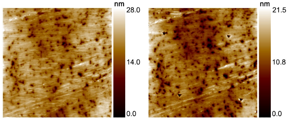
Figure 1 displays a representative 20 μm, 2D topographical in-situ SPM image that was acquired from Sample 2. Similar images acquired across the range of samples were used to determine surface roughness, which was in turn used to identify suitable sites for nanoindentation tests. Table 1 shows the three samples’ roughness after polishing. Table 1 also includes information on reduced modulus, hardness and wear depth.
Table 1. Hardness, reduced modulus, wear depth, and roughness on the polished surfaces of Sample 1, Sample 2, and Sample 3. Source: Bruker Nano Surfaces
| |
Hardness (GPa) |
Modulus (GPa) |
Wear Depth (nm) |
Roughness (nm) |
| Sample 1 |
30.65 |
437.41 |
60.567 |
2.00 |
| Sample 2 |
35.62 |
412.78 |
23.0735 |
2.60 |
| Sample 3 |
29.93 |
344.64 |
67.397 |
4.77 |
When testing a thin coating, it is standard practice to only test the first 10 % of the coating thickness, in order to prevent substrate effect on measurements. With this in mind, tests here were kept below 200 nm, because the coatings being investigated were approximately 2 μm.

Figure 1. In-situ SPM image of polished nitride hard coating showing pre-test (left) and post-test (right). Image scan size was 20 μm. Image Credit: Bruker Nano Surfaces
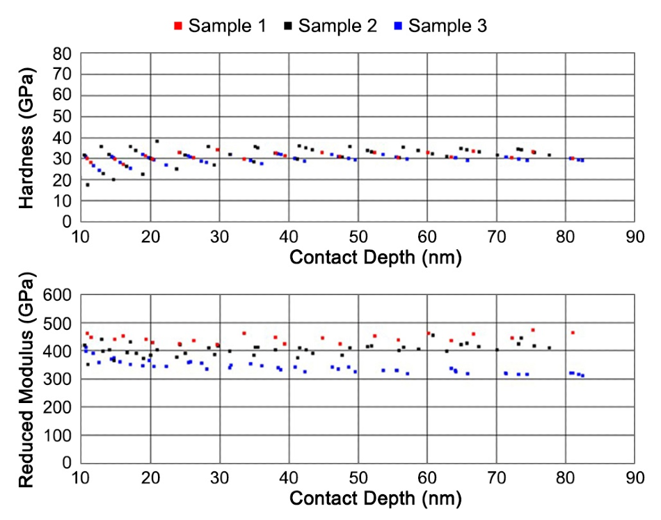
Figure 2 displays the reduced modulus and hardness for three hard coating samples at varying depths, from 10 nm to 90 nm. Because no trends in the hardness or modulus are seen with changing depth, the results can be considered to show the coating properties with no substrate effect.

Figure 2. Hardness and reduced modulus of hard coatings as a function of indentation depth. Image Credit: Bruker Nano Surfaces
The average value for reduced modulus and hardness is displayed in Figure 3. The results confirm that, of the three coatings, Sample 1 has the highest modulus, while Sample 2 has the highest hardness.

Figure 3. The average value of hardness and reduced modulus from indents on Sample 1, Sample 2, and Sample 3. Image Credit: Bruker Nano Surfaces
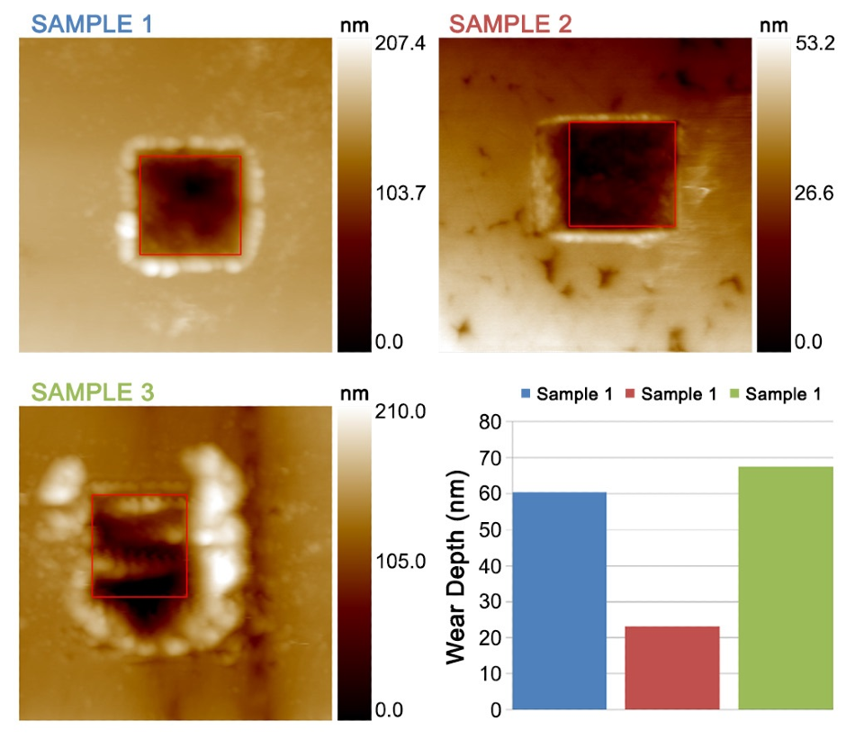
Figure 4 displays in-situ SPM images and measured wear of the three coatings after completion of ScanningWear tests. The squares represent the wear area, while the difference between mean height outside and inside each wear area is the wear depth.

Figure 4. 6x6 μm topographical in-situ images of the surfaces of Sample 1, Sample 2, and Sample 3 after wear tests on 2x2 μm areas at 400 μN with 20 passes. The chart shows the resulting wear depth for each sample. Image Credit: Bruker Nano Surfaces
Sample 2’s wear depth was measured as 23.07 nm --- considerably smaller than the other samples. Sample 2’s lower wear depth, therefore, indicates that it has the best wear resistance. Sample 2’s hardness was also found to be higher, indicating that there could be a correlation between wear resistance and hardness.
No correlation was measured between modulus and wear resistance, however. Large amounts of pile-up around Sample 3 suggest that the wear mechanism could have differed between Sample 3 and the other samples.
Conclusions
As can be seen above, a Hysitron TI Series nanoindenter was employed in the successful measurement of reduced modulus, hardness and wear depth for thin, super-hard coatings on steel samples. In-situ imaging was vital in the verification of sample roughness, as well as in test placement and post-test analysis.
Major substrate effects can occur for a hard coating on a soft substrate, so the ability to rapidly and automatically obtain mechanical properties as a function of depth enabled users to verify that substrate effects were minimal.
The level of sensitivity present in Bruker’s proprietary transducer enabled tests to be performed below 200 nm –- and as far down as 10 nm in depth --- with ease.
All these tests can be fully automated, making them easy to apply in both R&D and process control. Being able to characterize wear properties of ultra-thin films and to understand sliding single asperity contact interactions in conventional engineered systems is essential in the design of components which have an extended service life.
Acknowledgments
Produced from materials originally authored by Dr. Ude D. Hangen from Bruker.

This information has been sourced, reviewed and adapted from materials provided by Rigaku Corporation.
For more information on this source, please visit Bruker Nano Surfaces.