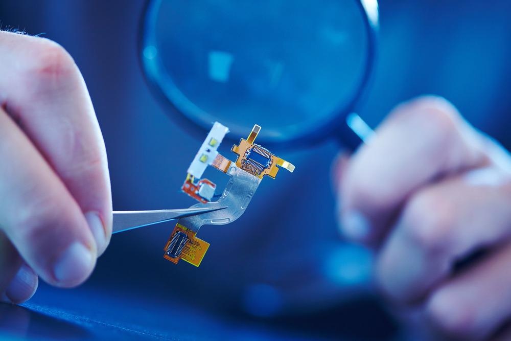
The demand for cost-effective but increasingly greater computing power over the last fifty years has driven research and development into new materials and processes to meet the demand. Devices have progressively been miniaturized increasing the electronic component density within these devices, and as a consequence this escalates an issue regarding thermal management of the resulting architectures.

Image Credit: allstars/Shutterstock.com
Without addressing thermal challenges, the effectiveness of emerging applications and the scope of their implementation will ultimately be limited.
Here, some of the state-of-the-art material processing that is producing some novel thermal conductors are considered, which could serve to obviate the possibility of overheating within future-generation electronics.
Hot Spots
Over time, integrated circuit devices, such as computer chips, have shrunk in size while transistor density has risen to such an extent that increasing power dissipation has become problematic.
In essence, more power in smaller and smaller spaces can lead to overheating, making the possibility of component degradation a reality. It is therefore a critical factor in determining the speed, efficiency, and reliability of electronic devices that they remain cool.
Thermal management and reliability implications are important. Today, heat loads approaching an excess of 1 kW for some processor modules are the result of the power requirements for many high-performance applications.
Power dissipation of such high magnitude, in combination with concerns about spatial distribution and non-uniformity across a die surface, means modern chip architectures can experience localized power-dense regions or “hot spots”, ranging anywhere from 500 mm2 up to 5 mm2 in size.
The power density can be a factor of up to ten times higher than the die average.
Given that the overall reliability of electronics is not determined by the average die temperature but rather the hottest region, surface non-uniformity exposes vulnerability in current material designs being adequately robust.
Anisotropic Materials
In the world of materials, those described as being isotropic typically possess property homogeneity.
This is where similar, quantifiable properties can be measured in all directions. Those that exhibit directional independence, that is, the measurement of different physical properties along different axes are known as anisotropic.
Investigating thermal conduction anisotropy within materials to remove hotspots is a relatively recent development in material science. In essence, if a material can be constructed that conducts and insulates heat in different directions at the micro scale, then hotspot removal and, as a consequence, thermal management of electronic components could be realized.
Find Out More About New Advances in the Electrical Field
In stacking and rotating thin crystalline layers, researchers have discovered the ability to direct heat flow, different thermal conductivities, along different crystal axes. In doing this, thermal conductivity anisotropy ratios between a fast axis along which heat flows faster in one direction than a slow axis are created.
What is driving research is that anisotropy ratios are very small amongst artificially engineered thermal conductors, and need to be larger if these of types of materials are to have any real impact in electronics generally, where next-generation technology nodes will demand 14 nm and below in terms of minimum feature sizes.
Material Criteria
In selecting materials suitable for real-world applications with the necessary higher anisotropy ratios, the architect must take into consideration a number of factors. First and foremost, the materials must be facile enough to allow precise control of their dimensions including film thickness, allowing in turn integration and scalability of production.
van der Waals (vdW) thin films have charge fluctuations resulting from the weakest intermolecular forces induced by dipole–dipole forces that repel each other strongly. These dispersion forces make them ideal candidate materials for application in the context described here.
In addition, candidate materials must exhibit innately high fast axis heat propagation while being produced by a method that substantially reduces slow axis phenomena, but not at the expense of fast axis properties. This is what makes the findings of Kim Shi En et al. exciting.

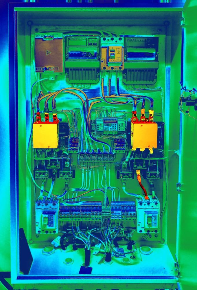
A thermographic image of an electrical cabinet shows areas at risk of overheating. Image Credit: Valery Lisin/Shutterstock.com
New Degree of Freedom
Using layered van der Waals (vdW) thin films of transition metal dichalcogenides (TMDs) as material platforms with intrinsically high in-plane thermal conductivities, Kim Shi En et al. have developed an approach for significantly decreasing the out-of-plane thermal conductivity while maintaining high in-plane conductivities of these materials in single-crystalline forms.
The molecular engineering of these crystalline structures involves interlayer rotations of TMD films and introduces a new degree of freedom for heat transport in solid-state systems.
The team have grown, at a large-scale, films using a technique known as metal-organic chemical vapor deposition.
Layer-by-layer stacking in vacuum of molybdenum and tungsten disulfide bilayers (MoS2 and WS2) upon silicon dioxide/ silicon (SiO2/Si) substrates has produced extremely anisotropic thermal conductors.
An Exceptional Thermal Anisotropy Ratio
By making random interlayer rotations, the through-plane or out-of-plane translational symmetry is broken at the atomic scale while retaining in-plane long range crystallinity in each monolayer. In effective, it allows the impediment of the through-plane thermal transport while the long-range intra-layer crystallinity maintains high in-plane thermal conductivity.
Out-of-plane, in other words, is suppressed. As a result, the group has recorded one of the greatest ever thermal anisotropy ratios in MoS2, nearly 900 at room temperature, quantitatively rationalizing these values using molecular dynamics simulations. It is a significant advance within the field.
Further Research
The new materials are promising, but for their wide adoption into electronic devices to really occur, much still needs to be done.
Their true viability still needs exploration. Scalable manufacturing, performance reproducibility and compatible coefficients of thermal expansion are among some of the more considerable challenges facing those keen for their exploitation.
For success at the industrial scale, improved quality, reduced cost and maintained uniformity are all pre-requisites. Moving this fascinating area of material science forward would be a game-changing step in the synthesis of more highly conductive materials.
The incorporation of 3D foam structures into chip stacks, for example, holds possibilities for thermal management, provided signal integrity can be sustained and shorting avoided.
References and Further Reading
Kim Shi En et. al. (2021). Extremely anisotropic van der Waals thermal conductors. Nature 597, 660 https://doi.org/10.1038/s41586-021-03867-8
Minnich, A. J. (2016). Exploring the extremes of heat conduction in anisotropic materials Nanoscale Microscale. Thermophys. Eng. 20, 1 https://doi.org/10.1080/15567265.2016.1170080
Cui, Y. et. al. (2020). Emerging interface materials for electronics thermal management: experiments, modeling, and new opportunities. J. Mater. Chem. C 8, 10568 https://doi.org/10.1039/C9TC05415D
Moore A. L. et. al. (2014). Emerging challenges and materials for thermal management of electronics. Materials Today 17(4), 163 https://doi.org/10.1016/j.mattod.2014.04.00
Disclaimer: The views expressed here are those of the author expressed in their private capacity and do not necessarily represent the views of AZoM.com Limited T/A AZoNetwork the owner and operator of this website. This disclaimer forms part of the Terms and conditions of use of this website.