Parylene offers a robust combination of high dielectric strength, low coefficient of friction, high operating temperature and biocompatibility – features that make parylene an appealing choice of material in the electronics industry.
Parylene stands out from other conformal coating technologies due to its distinct gas phase polymerization and deposition process.
Conventional conformal coatings are generally applied in the liquid phase via dipping, brushing or spraying the components.

Figure 1. Schematic representation of a typical polymerization and deposition process for perylene N conformal coatings. Calculated thickness determined using an FFT-based algorithm. Image Credit: Avantes BV

Figure 2. Comparison of liquid and parylene conformal coatings. Image Credit: Avantes BV
Liquid phase coatings are appropriate for low-end applications, but these coatings remain susceptible to localized air pockets and variations in coating thickness that can lead to coating defects (Figure 2).
Parylene coatings can be applied via a three-step vapor deposition polymerization (VDP) process (Figure 1).
This process is like traditional chemical vapor deposition (CVD). Powdered di-para-xylylene is vaporized at 1500 °C, and once this has entered its gas phase, the dimer moves into a second tank where it is heated to the point of pyrolyzation.
The dimer splits at this point, forming individual monomers. The resultant mono-para-xylylene gas moves into a third tank. The component of interest is held at 25 °C, filling every crack and crevice as the gas adheres to the surface to form a thin epitaxial polymer coating. This process coats one molecule at a time.
It is important to note that because the coating process occurs at room temperature without the use of further curing, the substrate is not subjected to additional stresses and strains. This can also be considered a relatively ‘green’ process because polymerization takes place without any catalysts or solvents.
The use of gas-phase epitaxial growth results in extremely uniform coatings with excellent penetration of crevasses.
Coating thickness is only limited by processing time. For example, the expected coating rate of parylene C is around 3-5 microns per hour. Standard coating thicknesses tend to range from 500 angstroms to over 75 microns.
Measuring parylene thickness is, therefore, one of the most crucial factors in ensuring coating process quality.
A wide range of high-end methodologies is suitable for determining coating thickness, for example, scanning electron microscopy (SEM) and white light confocal microscopy.
The best balance between size, cost and complexity can be achieved with reflectance spectroscopy, however, particularly when used in widespread quality control applications.
Measuring Coating Thickness: A Case Study
When spectroscopy is used to investigate thin film coatings, a portion of the light will be reflected and transmitted whenever light passes between materials.
Thin film coatings can be considered in terms of a simple Fabry-Perot resonator, whereby light reflected off the top and bottom layers will either constructively or destructively interfere based on the relative phase difference.
Phase difference, in this case, is determined by the material’s optical path length, which will be equal to the refraction index of the coating times twice the coating thickness.
Knowledge of the material’s index will therefore enable the straightforward determination of its thickness. The only caveat to this approach is that the index of refraction is a wavelength-dependent complex function of refraction: n^* (λ)=n(λ)+ik(λ), where n is the index of refraction, and k is the absorption coefficient.
Avantes has addressed this potential issue by compiling an extensive library of n and k values for the majority of common coating materials, including parylene.
Figure 3 displays the reflectance spectra of a test coupon with a 7-micron parylene C coating. By evaluating the frequency chirp in the reflectance spectrum, it was possible for the third-party thin film software (created by Boulder Optical Design) to determine the precise thickness to be 6.81 +/- 0.08 microns.
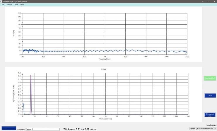
Figure 3. Reflectance spectra of a 7-micron parylene C coating, along with the calculated thickness determined using an FFT-based algorithm. Image Credit: Avantes BV
Data in this example was acquired using the Ava-Reflector, currently only available from Avantes USA (Figure 4).
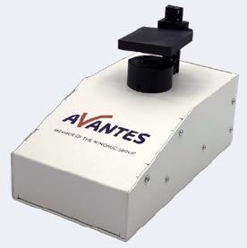
Figure 4. Ava-Reflectometer System. Image Credit: Avantes BV
This system features Avantes’ Avalight-HAL-S-Mini2 halogen light source, a miniature reflection probe, and the AvaSpec-Mini-2048CL. These components are housed in a single compact, easy-to-use thin film measurement device.
The Ava-Reflectometer is a lightweight (2.27 Kg) thin-film spectro-photometer that features a maximum spectral range of 200 nm to 1100 nm. This compact instrument facilitates the straightforward measurement of opaque or transparent substrates coated with thin films.
Equipment Options and Instrumentation
Users seeking a more modular setup can benefit from Avantes’ portfolio of thin-film measurement bundles.
Each of these includes a fiber-coupled spectrometer, such as the AvaSpec-Mini2048CL (Figure 5) or AvaSpec-ULS2048CL-EVO (Figure 6); a fiber-coupled deuterium halogen or constant current tungsten light sources, such as the Avalight-HAL-S-Minis (figure 7) or AvaLight-DHc (Figure 8), and a fiber-optic reflection probe such as the FCR-7UV200-2-ME (Figure 9).
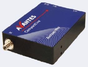
Figure 5. Avaspec-Mini2048CL. Image Credit: Avantes BV
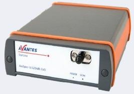
Figure 6. AvaSpec-ULS2048CL-EVO. Image Credit: Avantes BV
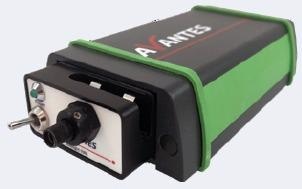
Figure 7. Avalight-HAL-S-Mini. Image Credit: Avantes BV
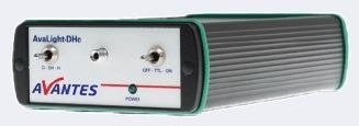
Figure 8. AvaLight-DHC. Image Credit: Avantes BV
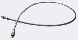
Figure 9. Avantes Fiber Cable. Image Credit: Avantes BV
Avantes can also supply users with the AvaSoft Thin Film software add-on. This facilitates two methods of thin-film calculation: Fast Fourier Transform (FFT) and best-fit optimization algorithms.
The FFT method allows users to determine the interference pattern frequency, allowing them to employ the n and k values to calculate the corresponding thickness. This algorithm is well suited for working with thicker coatings that exhibit relatively high-frequency chirps.
Spectral matching is able to predict the best fit based on a series of adjustable fitting parameters, making this method ideal for thinner coatings with comparatively low-frequency spectral chirps or for use in applications that would benefit from high-speed monitoring.
Conclusion
Spectral reflection can be used to measure the thickness of any optically transparent coating.
Avantes has a long history of providing fiber-coupled miniature spectrometers, probes and light sources which can be combined with the company’s AvaSoft Thin Film software module to achieve single-layer thin film measurements from 10 nm to 100 μm thickness with 1 nm resolution.
Expanding its portfolio with the Ava-Reflectometer instruments allows Avantes to support thin film thickness measurements at any stage of the quality control process, from offline test coupon analysis to automated inline testing.
The company’s Avaspec instruments can be employed in high-speed triggered or continuous measurements, for example, those required in the application presented.
Avantes’ complete range of spectrometers is available as OEM modules suitable for integration into the multichannel rack mount systems commonly found in thin-film process monitoring systems.
These units offer a range of communication and interface options, including Ethernet, USB and the native digital and analog input/output capabilities of the Avantes AS7010 electronics board.
The Avantes AvaSpec DLL software development package includes samples programs written in Visual Basic, C#, C++, Delphi, LabView, MatLab and a number of other programming environments. This software development kit empowers users to develop their own code for thin-film applications.
It is beneficial when looking to integrate an instrument into an automated sampling system or when the analysis of sophisticated multi-layer thin films necessitates the use of a customized code.

This information has been sourced, reviewed and adapted from materials provided by Avantes BV.
For more information on this source, please visit Avantes BV.