Sponsored by Element SixReviewed by Emily MageeJul 29 2024
Energy-efficient electronics now have new possibilities, thanks to an innovative diamond-enabled microscope that is making quantum metrology portable.

Image Credit: Element Six
The first commercially produced microscope to incorporate diamond nitrogen-vacancy (NV) centers for quantum technology is Qnami's ProteusQ™. It allows for atomic-level tabletop examination of magnetic materials using a method known as scanning NV magnetometry.
This recently developed, diamond-enabled microscope provides a previously unheard level of miniaturization for operations that once required light sources with a circumference of many hundreds of meters.
This widely available technology lowers the technical barriers for studying nano-scale materials and is anticipated to accelerate the creation of advanced materials for devices that use less energy.
Element Six has been at the forefront of synthetic diamond innovation for decades. For Qnami, Element Six has been both a technical partner with whom we develop new applications and a reliable source of high-quality diamond for our production needs.
Dr Mathieu Munsch, Chief Executive Officer, Qnami
The Opportunity: A New Generation of Energy Efficient Electronics
The magnetic characteristics of materials for electrical devices had previously received modest attention. Spintronics, a new branch of electronics category, promises to combine high performance with minimal environmental impact. In spintronics, information is recorded in magnetic bits in spintronics, exactly as in conventional hard disc drives.
An electron’s spin, a quantum property, can be utilised to convey information in place of its charge, allowing it to move on spin-waves rather than electrical current.
The Challenge: Big Science with Atomic Precision
Complex thin film structures or multi-layers, whose thickness must be regulated down to one atomic layer, are needed for spintronics. Further engineering transforms these films into intricate nano-structures with lateral sizes as small as a few nanometres.
It is vital to measure the consequences of microscopic modifications in the design or fabrication process to determine the main cause of any system malfunctions. Traditional diagnostic methods, however, do not directly reveal the magnetic characteristics of such devices, delaying development.
Existing Technology: X-Ray Magnetic Circular Dichroism
The current technique for spintronics precise metrology, X-Ray magnetic circular dichroism (XMCD), needs extremely large synchrotrons, which can be hundreds of meters across and are operated by large teams of people. In a fast-paced research or production context, getting access to such a facility and resources might be expensive, time-consuming, and - overall - not feasible.
Why Diamond?
The potential for highly sensitive sensors to measure magnetic and electric fields is enormous, given the exceptional fragility of quantum states. However, the exceptional fragility of quantum states also poses a significant problem. Quantum states would ideally be separated from their surroundings to minimise noise and interference, but - at the same time - measurement necessitates some degree of external interaction.
The narrow line quantum engineers are increasingly motivated to cross to fully use this intriguing technology represents the balance between control and interaction. Synthetic diamond is an ideal host material for spin qubits due to its stability and ease of qubit initialisation at room temperature.
Element Six (E6) CVD Single Crystal Diamond
- With its high sensitivity, extended decoherence times, and wide dynamic range (and vector functionality), E6's single crystal CVD diamond is the ideal spin qubit host material.
- Over the past decards, Element Six has invested time and resources to expand its innovation capabilities and further establish its broad patent portfolio in relevant areas related to quantum technologies.
- A variety of CVD diamond grades and other highly engineered, super abrasive materials are developed by Element Six for applications in machining, optics, thermal management, and sensing.

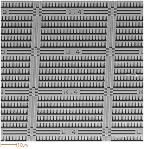
Diamond wafer during the manufacturing process of Qnami Quantilevers™. Image Credit: Qnami
Qnami and Element Six’s Solution: Scanning NV Magnetometry
With just one operator using the tabletop Qnami ProteusQ™, faster and more precise atomic-scale material investigation can now be carried out in a typical lab setting owing to the quantum power of NV diamond.
Using the Scanning NV Magnetometry method, sharp, microscopic quantum sensors with NV diamond tips can be manipulated with extreme precision over minute magnetic structures to map and visualise magnetic properties. This solution ten times better than large-scale XMCD and provides increased spatial resolution at the scale level.
This advanced diamond-enabled device can speed up the R&D and commercialization of new technology that depends on nano-structures and the manipulation of electrons by providing real-time feedback, unlocking the possibility of industrial scaling.
What is a Nitrogen Vacancy (NV) Center?
Pioneering research from Harvard University and the University of Stuttgart showed that carbon atoms with nitrogen vacancy centers, a defect also present in some rare pink nateral diamonds, have a quantum spin that can be controlled and read out at room temperature using standard optical methods.
With unprecedented levels of accuracy, these quantum defects can be engineered by Element Six into synthetic diamonds that are manufactured using their proprietary chemical vapor deposition (CVD) processes and technology.
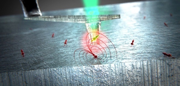
NV centers are color centers in which a nitrogen atom replaces a carbon atom, leaving a vacancy (or missing carbon atom) in its place. Technology for sensing and magnetometry is based on the NV’s electron spin, which is extremely sensitive to magnetic fields.
Since the electron spin can be easily detected and read out by simply shining a green LED on the material and gauging the amount of red fluorescence it emits, this platform is extremely and practical.
At room temperature, it has been shown that NV electron spins can store quantum information for more than 1 millisecond. For some applications, ensembles of several NV centers are necessary. Still, this method of detection and alignment can also be used with a single NV center, creating new opportunities for groundbreaking spatial resolution and nano-scale sensitivity.
Next Steps: Commercial Spintronics
With the introduction of Magnetic RAM (MRAM) technology, spintronics is transitioning from the lab to creating commercial products. A growing variety of prospects, based on a new generation of sophisticated semiconductor materials, such as ultra-thin ferromagnets, antiferromagnets, multiferroics, and 2D materials, is envisaged to be made possible by the significant advantages provided by Scanning NV Magnetometry.
The next task will be to scale down even further to deliver increasingly more portable solutions and further develop the materials characteristics to enable the measurement of multiple physical properties under different circumstances.
Element Six has worked with this technology back when it was still basic science in Harvard over ten years ago. Today it is incredibly exciting to see this ground-breaking science coming to fruition and we are proud to collaborate with Qnami in the commercialization of a new solution that will enable crucial breakthroughs in spintronics materials.
Dr Daniel Twitchen, Executive Director, Business Development & Technologies Sales, Element Six

Artists rendering of a diamond Quantilever™ containing a single NV center for high-resolution quantum imaging. Image Credit: Element Six

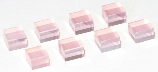
Element Six’s DNV-B1™-the first commercially-available, general-purpose quantum grade diamond. Image Credit: Element Six

This information has been sourced, reviewed and adapted from materials provided by Element Six.
For more information on this source, please visit Element Six.