Sponsored by CSEMReviewed by Maria OsipovaMar 8 2023
One of the most promising new materials for photonic integrated circuits (PICs) is lithium niobate on insulator (LNOI). This platform offers a variety of unique optical characteristics, including a high electro-optic (EO) coefficient, high intrinsic 2nd and 3rd order optical nonlinearities, and a large transparency window (350 to 5500 nm).
The purpose of this project is to expand CSEM's expertise in various aspects of the value chain, including PIC design, simulation, fabrication, photonics packaging, testing, and the creation of a functional experimental demonstration.
With the maturity of the technology, it is now possible to integrate a detector for carrier-envelope frequency offset, which is crucial for stabilizing femtosecond lasers. The successful completion of this demonstration will validate CSEM's ability to deliver a fully packaged and competitive PIC-based solution, from design to final product.
This project utilizes CSEM's multidisciplinary expertise in Photonic Integrated Circuit (PIC) design and fabrication, packaging, system engineering, laser stabilization, and metrology to construct a full demonstration of a Carrier-Envelope Offset Frequency (fCEO) detection unit.
The fCEO detection unit, based on Lithium Niobate on Insulator (LNOI) waveguide technology,1 requires a lower optical pulse energy and results in a smaller, more cost-effective solution compared to the traditional approach utilizing highly nonlinear fiber and frequency doubling crystal.
These advantageous characteristics have the potential to greatly enhance the use of optical frequency combs in various industrial and space applications by reducing costs, size, and power consumption.
The demonstration unit is constructed using a low-loss etching technique for Lithium Niobate on Insulator (LNOI) waveguides, which have proven to be reliable under femtosecond pulse illumination1 and have exhibited low loss levels of less than 0.2 dB/cm.
Currently under development, a two-level waveguide etching process will enable the creation of a double-inverse taper necessary for efficient light coupling between the optical fiber and the LNOI waveguide. The goal is to achieve a loss of less than 1 dB per facet, with current results showing a loss of 4 dB per facet.
In addition to the fiber and LNOI waveguide, the demonstration unit includes a photodiode placed at the waveguide output to detect the fCEO signal.
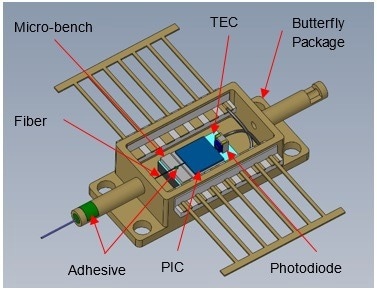
As shown in the CAD design presented in Figure 1, the components can be housed within a standard butterfly 14-pin package, which is mounted on a Peltier element serving as a micro-bench. The unit is also designed for hermetic sealing.

Figure 1. CAD design for the demonstrator. Image Credit: CSEM
An important challenge in the packaging process is the precise bonding of the optical fiber to the waveguide, as the mode field diameter is small (around 3 µm), requiring tight tolerances in the fiber's position.
The project represents a critical step towards CSEM's goal of becoming a strategic partner in photonic integrated circuit (PIC) device development, encompassing the entire value chain from design and fabrication to system integration.
CSEM is actively seeking additional partnerships for industrial-grade packaging implementation.
LNOI PIC technology offers unparalleled potential, with its unique characteristics, to impact a range of applications such as laser technology, telecommunications, sensing, and quantum.
References
- E. Obrzud, et al., (2021) Stable and compact RF-to-optical link using lithium niobate on insulator waveguides. APL Photonics, 6, p. 121303.

This information has been sourced, reviewed and adapted from materials provided by CSEM.
For more information on this source, please visit CSEM.