Spectroscopy, a branch of the physical sciences, investigates the interactions between electromagnetic radiation and matter. It involves analyzing how light interacts with a sample—whether through absorption, reflection, transmission, emission, or scattering. Additionally, spectroscopy can be used to study a sample’s fluorescence.
The field of spectroscopy is broad and can be categorized by the wavelength range of light examined, encompassing various types such as infrared, visible, microwave, and X-ray spectroscopy.
Hamamatsu Photonics provides a comprehensive portfolio of high-performance components and modules tailored for both the near-infrared (700-2500 nm) and visible (300-700 nm) ranges. Its products are increasingly popular across diverse application areas, including environmental monitoring, chemical analysis, and material testing.
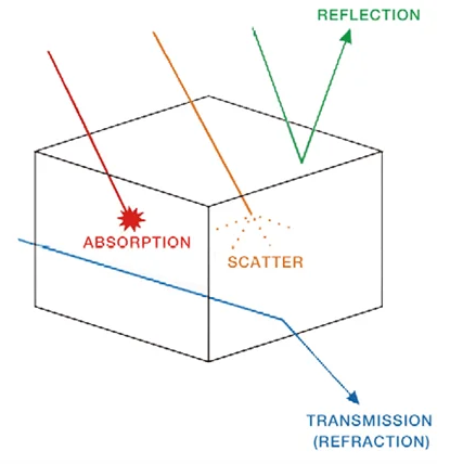
Figure 1. Types of spectroscopy. Image Credit: Hamamatsu Photonics Europe
In visible spectroscopy, absorption involves atoms and molecules absorbing visible light through electronic transitions. As an atom or molecule absorbs light of a specific wavelength or energy, this will lead to a decrease in the amount of transmitted light.
In liquids and solids, visible light is mainly absorbed by the presence of conjugated double bonds and aromatic rings within organic molecules. Transition metal ions in aqueous solutions can also create strongly absorbing species through their interactions with water molecules in visible light absorption.
The wide range of colors observed in condensed phases results from the absorption of light via electronic transitions, which generates an extensive spectrum of colors.
Light in the near-infrared (NIR) spectrum does not have enough energy to induce the electronic transitions seen in the visible range. Consequently, compounds that are brightly colored in the visible range have minimal effect on NIR absorption.
Instead, in the NIR range, light is absorbed through vibrational transitions. When light has the right energy or wavelength, it can enhance vibrational modes between atoms within a molecule.
NIR absorption differs from visible absorption as it does not require conjugated bonds or solvent complexes but rather depends on the molecule’s specific structure and its interactions with surrounding molecules.
This sensitivity to molecular structure and environment is a key advantage of NIR spectroscopy, with Raman scattering being one of its most important techniques.
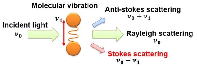
Figure 2. The principle of Raman spectroscopy. Image Credit: Hamamatsu Photonics Europe
Raman spectroscopy analyzes the vibrational modes of the molecules or crystals in question. As light is directed at a material, some of this will be scattered. This scattered light either exhibits an identical wavelength to the incident light (Rayleigh scattered light) or differing wavelengths (Raman scattered light).
Raman spectroscopy examines the properties of this Raman scattered light, allowing users to identify the molecular or crystal structure of substances. This technique is well suited to the analysis of the majority of substances with no need for pre-treatment. It can also be used to investigate organic matter, inorganic compounds, liquids, solids, gases, and more.
Raman spectroscopy works by measuring the Raman shift, which can be understood as the energy shift that takes place during Stokes scattering. Stokes scattering is much less likely to occur than Rayleigh scattering, however.
It is also important to note that Raman spectroscopy is a ‘fingerprint technique’ that is able to provide rich, diverse information based on the unique spectral signatures produced by each specific substance.
One popular application of Raman spectroscopy lies in authenticating historical art, where it is employed in the analysis of paint’s crystalline or molecular structure to verify a piece’s authenticity.
Raman spectroscopy is also widely used in the semiconductor industry, where it is employed in the analysis of crystalline samples; and in the chemical and pharmaceutical industries where its ‘point-and-shoot’ nature and lack of sample pre-treatment requirements makes it a popular choice.
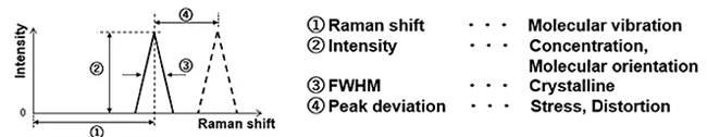
Figure 3. Four Raman spectroscopy categories. Image Credit: Hamamatsu Photonics Europe
The first category involves the Raman shift, which offers general insights into the crystal or molecular structure of the sample. The second category pertains to intensity, which reflects the concentration of the various substances present.
The third category assesses the full width at half maximum of the peak and examines its shape to provide information about the crystalline structure.
Finally, any deviations in the peaks might reveal interactions with neighboring molecules or result from distortions and strain within the molecular structure. This is illustrated by the spectrum representing the different states of water, as depicted in Figure 4.
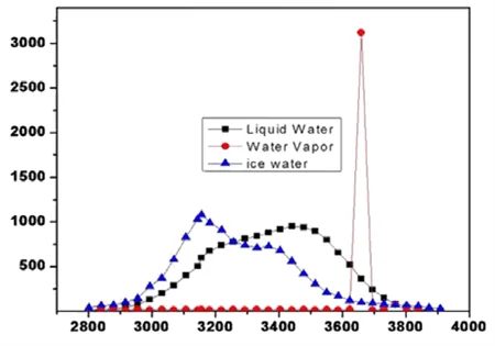
Figure 4. Spectrum of different states of water. Image Credit: Hamamatsu Photonics Europe
Figure 4 illustrates that the Raman spectrum of water vapor shows a sharp peak, while liquid and frozen water produces much broader peaks. This difference is due to the varying molecular interactions with surrounding molecules in each state.
A notable advantage of Raman spectroscopy is that the energy shift observed is unaffected by the incident wavelength. This allows Raman spectroscopy to be applied across a wide range of energy levels.
Common wavelengths used in Raman spectroscopy include those from standard semiconductor diode lasers, such as 532 nm, 785 nm, and 1,064 nm.
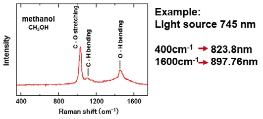
Figure 5. Intensity measurement of methanol. Image Credit: Hamamatsu Photonics Europe
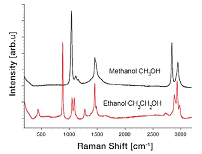
Figure 6. Comparison of the Raman spectrum of pure Methanol and Ethanol. Image Credit: Hamamatsu Photonics Europe
The spectra shown in Figures 5 and 6 exhibit similar peaks corresponding to the same wavelength, but it can be observed that ethanol has other distinct peaks. Ethanol is a larger molecule, meaning that it possesses more vibration modes that can be excited by Raman spectroscopy.
It should also be noted that the examples shown here display high-quality Raman spectra with exceptional spectral resolution and signal-to-noise ratio. Obtaining such high-quality spectra is typically difficult to achieve because the low probability of Stokes scattering versus Rayleigh scattering is larger due to factors of millions to billions.
A standard Raman spectroscopy setup typically comprises three essential components: a coherent light source, usually a laser; optical elements such as mirrors, filters, and gratings; and a sensitive detector for capturing the Raman scattered light.
However, the visible and near-infrared parts of the spectrum are typically of concern in Raman spectroscopy, and a detector with high sensitivity is needed to detect the extremely faint Raman scattered light. Linear image sensors are frequently used for this purpose to detect multiple dispersed wavelengths simultaneously.
Hamamatsu Photonics is a prominent provider of high-quality, high-performance, and cost-effective CMOS technology for analytical, industrial, and spectroscopy applications. Leveraging its extensive expertise in photonics, including optics, mechanics, electronics, and software, Hamamatsu offers a diverse range of products, such as CCDs (including TDI-CCDs), CMOS sensors, and NMOS sensors.
The latest CMOS linear image sensor from Hamamatsu, the S16596-4096-11, enhances the features of previous models. It features an extended pixel size of 7x200 μm, a resolution of 4096 pixels, a maximum data rate of 10 MHz, low readout noise (typically 0.4 mV rms), and a high dynamic range of 5000 times.
This sensor includes important functions like simultaneous charge integration across all pixels, adjustable integration times, an integrated timing generator, and an electronic shutter. The S16596-4096-11 sensor delivers improved sensitivity, making it highly suitable for Raman spectroscopy applications.
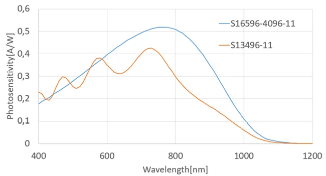
Figure 7. Comparison with the previous model. Image Credit: Hamamatsu Photonics Europe
In addition to the sensor, Hamamatsu also provides a driver circuit that features a 16-bit digital output and is compatible with USB 2.0 interfaces. The power for the driver circuit can be supplied through the USB bus, with a DC+5V requirement. The driver circuit supports a readout frequency of 10 MHz. The Sensor Board dimensions are 20 x 41.6 mm, while the Interface Board measures 45 x 50 mm.
The driver circuit also supports external synchronization, offering greater flexibility for various applications.
For testing and evaluation purposes, Hamamatsu offers an evaluation board that includes both the sensor and readout boards, as well as a lens mount (F-mount), allowing users to assess the CMOS sensor’s performance in specific applications. Boards and a lens mount (F-mount) can be provided to allow testing of this CMOS for a specific application.
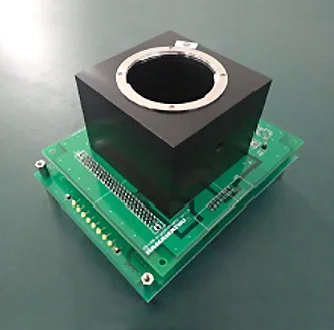
CMOS linear image sensor, S16596-4096-11. Image Credit: Hamamatsu Photonics Europe
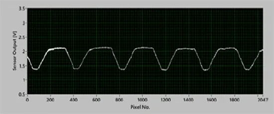
Figure 8. Typical output of the readout board The vertical axis indicates the sensor output. The horizontal axis indicates the number of pixels. Image Credit: Hamamatsu Photonics Europe
Acknowledgments
This information has been sourced, reviewed and adapted from materials provided by Hamamatsu Photonics Europe.

This information has been sourced, reviewed and adapted from materials provided by Hamamatsu Photonics Europe.
For more information on this source, please visit Hamamatsu Photonics Europe.