|
CeramTec is a leading manufacturer of alumina and aluminum nitride substrates. More than 30 years of production experience as well as a strong global commitment, including manufacturing sites and laser facilities in Europe, North America and the Far East, enable CeramTec to be a resourceful and dependable partner for the microelectronic industry and other manufacturers of electronic components.
CeramTec’s Rubalit® alumina and Alunit® aluminium nitride materials were developed in our own laboratories. Continuous material improvement is achieved by applying the latest quality methods, such as SPC, DOE, FMEA, etc.
CeramTec has developed state-of-the-art manufacturing technologies for substrates, including tape casting, sintering, lasering, stamping, dry-pressing, as well as metallization of ceramics.
Lasered Substrates with Tight Tolerances
Lasered substrates are characterized by very tight tolerances and enable a variety of outside geometries, contours, hole combinations and scribe lines.
No tooling is involved in lasered substrates. This lowers production lead-time and cost.
Data Transfer via CAD
Customers can transfer their data directly via long-distance data lines. This guarantees higher dependability and accuracy while shortening lead-time.
Complex Geometries and Precision Holes
With the aid of computer controlled CO2 lasers, Rubalit® alumina and Alunit® aluminium nitride substrates can be:
- scribed
- machined
- drilled
- notched
Smallest Hole Diameter
Holes as small as 0.08 mm (0.00032") can be machined into Rubalit® alumina and Alunit® aluminium nitride substrates.
Metallized Rubalit® Alumina and Alunit® Aluminum Nitride Substrates
Ceramic substrates, with their excellent mechanical, electrical and thermal characteristics, are metallized on-site in our facilities. The metallization types developed by CeramTec enable superior adhesion, wettability, and excellent performance consistency in soldering baths.
Layer Design
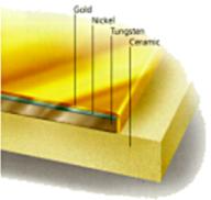
The base layer is tungsten, screenprinted with minimum layer thickness of 6 µm. An electroless nickel layer (approximately 2 µm) assumes a good solder flow. Other thicknesses are available for specific customers' requirements.
Electrolytic nickel plating requires electrical connections during plating. Therefore, special design guidelines apply if electrolytic technology is required.
An additional gold flash layer (approximately 0.11 µm) can be added to enhance corrosion resistance. Also, the electrolytic nickel layer can be covered with a bondable gold plated layer. Solder finishes are also available.

Figure 1. Refractory Metallization System
Substrate Dimensions
For metallized substrates, the maximum standard dimension is 120 mm x 160 mm (4.7" x 6.3") for Rubalit® alumina and 115 mm x 115 mm (4.5" x 4.5") for Alunit® aluminium nitride. It is cost-effective to design the dimensions of the smaller, single substrate segments for maximum utilization of these master substrates.
Specifications
Metallized substrates are tested in accordance with CeramTec’s test procedures as well as with MIL STID 105, DIN, and ASTM standards.
In addition to dimensional verification, camber and layer thickness testing, solder wettability and adhesion are evaluated as well.
|