| Pulsed laser deposition (PLD) was first reported in 1965 to investigate the deposition of thin films of a variety of materials including semiconductors, dielectrics, organometallics and chalcogenides. However, it is only recently with the success of the technique for the deposition of high temperature superconductors that it has been widely accepted. The ability to deposit almost any material, preserve the stoichiometry of multi-component compounds and carry out reactive deposition has finally been recognised and renewed interest in this technology has been sparked in both academic and to some extent industrial organisations. Although the technique is simple in concept no one quite understands how and why it works so well. The Process A typical setup for depositing coatings by PLD is illustrated in figure 1. A laser pulse enters the vacuum chamber through a window and impinges onto the target of material to be deposited. The pulse is about 20-30ns wide with an energy density of about 1-10J.cm-2. It vapourises the target material in the form of a plume containing neutral, ionic and molecular species, which have a kinetic energy of a few electron volts. These then travel towards the substrate and deposit in the form of a thin film. About 1Å is deposited with a 200mJ pulse at 1-100 Hz with a vacuum of 100mtorr. As mentioned earlier, PLD is conceptually very simple. However, it involves a number of complicated interactions between the process variables such as wavelength, power density, background gas, pressure, target composition, substrate to target distance, substrate temperature, substrate bias and gas-surface interactions. These factors are currently under extensive investigation by researchers all over the world. A fuller picture of the process is finally emerging. A number of in situ diagnostic techniques such as time-of-flight mass spectrometry and optical emission spectroscopy are being used in an attempt to understand the plume composition and its relationship to the final film properties. For a detailed description of the process, considerable multidisciplinary effort in understanding the combined equilibrium and non-equilibrium processes involved will be required. Although PLD is widely claimed to be a low temperature technique, temperatures around 700°C are required to deposit high quality crystalline films. | 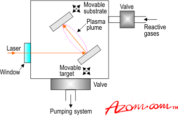
| | Figure 1. Schematic of the apparatus used for PLD coatings. | Coating Structures As far as the end product is concerned, the ability to deposit and precisely control the composition of 2, 3, 4, 5, or 6 elements at high partial pressures of reactive gases has resulted in the fabrication of novel electronic structures. The diversity and the power of the technique can be illustrated by the variety and the number of materials deposited. Over 100 materials have been successfully deposited in thin film form using PLD. In addition, it is relatively easy to deposit multi‑layers by substitution of targets into the path of the laser beam. An automated system can be designed easily employing known and proven sample/target handling devices. In a commercial set up the ability to timeshare a laser among a number of deposition/analysis chambers is attractive. The real deposition time when the laser is being utilised may be small compared to setting up, pump down and vent times. The laser beam can be readily steered from chamber to chamber. This reduces capital costs. It has also been shown that laser/target combinations can in some applications replace MBE cells. With progress made in using lasers for patterning, diffusion, annealing, doping, and laser induced chemistry it is therefore not hard to imagine the possibility of fabricating complete heterostructure based devices in situ using PLD type technologies. Applications PLD has been used to produce coatings for: • Biomedical applications • Solar cells • Superconductors Such coatings have been deposited at a rate of up to 1.5µcm2/sec, which is faster than is possible compared to other coating techniques such as physical vapour deposition (PVD) and chemical vapour deposition (CVD). |