Updated by Reginald Davey 16/01/2024
The superior heat capacity of tin makes it an ideal material for several important industrial applications. This, along with its good electrical, physical, and chemical properties, makes tin and its oxides such as tin dioxide (SnO2) an interesting candidate for semiconductor research.

Image Credit: RHJPhtotos/Shutterstock.com
Tin Dioxide: Overview of the Material
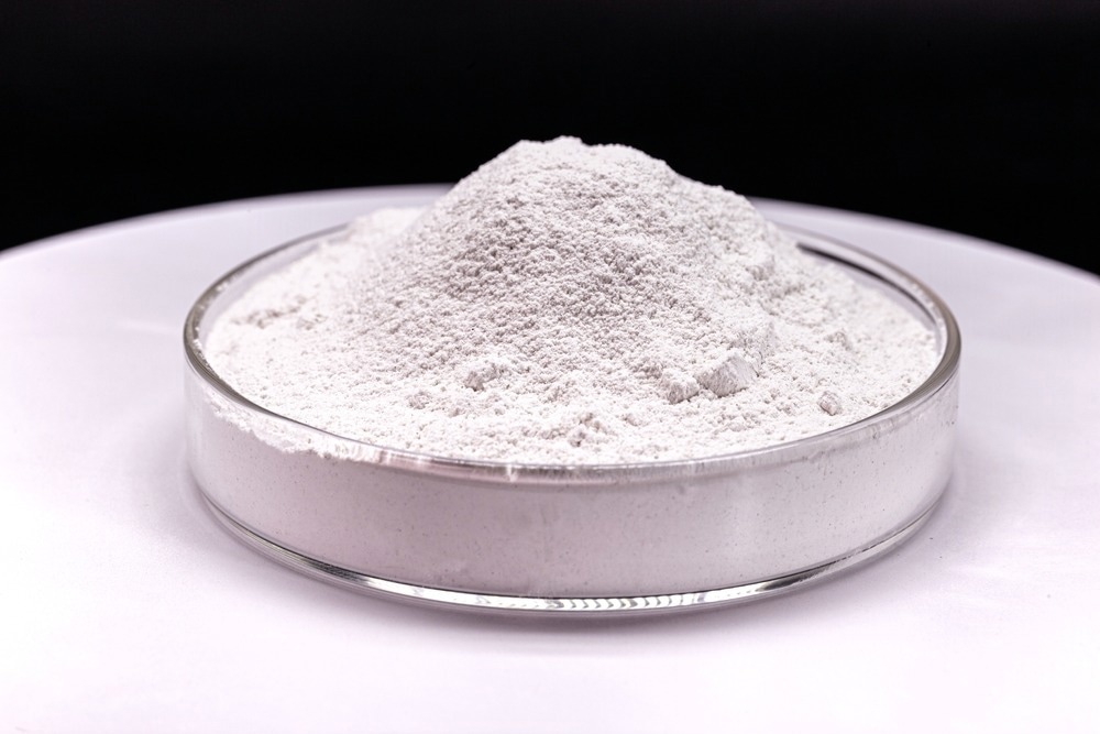
Tin dioxide (SnO2) is an inorganic compound with the chemical formula SnO2. It mainly occurs in the mineral cassiterite, and crystallizes with a tetragonal structure. It is a colorless, amphoteric and diamagnetic solid that is usually thought of as an oxygen-deficient n-type semiconductor.
SnO2 has different solubility in various solvents, being insoluble in water, but soluble in alkalis and acids. Reducing tin and burning it in air produces purified tin dioxide.
Applications
Tin dioxide finds applications in the following areas:
- Carbon monoxide detectors
- Catalysis for the oxidation of aromatic compounds
- Coatings and polishing powders
- Ceramic glazes.
Chemical Properties
The chemical properties of tin dioxide are provided in the table below:
| Chemical Properties |
| Chemical Formula |
SnO2 |
| Molecular Weight |
150.709 |
| CAS No. |
18282-10-5 |
| Group |
Tin – 14
Oxygen - 16 |
| Crystal Structure |
Tetragonal |
Electrical Properties
The electrical properties of tin dioxide are provided in the table below:
| Electrical Properties |
| Dielectric Constant |
9.86 |
| Band Gap |
3.57 eV |
Thermal, Mechanical and Optical Properties
The thermal, mechanical and optical properties of tin dioxide are provided in the tables below:
| Thermal Properties |
| Heat of Formation |
-280.7 kJ/mol |
| Standard Molar Entropy |
57.2 J/mol K |
| Specific Heat Capacity |
44.3 J/mol K |
| Mechanical Properties |
| Density |
6.9 – 7 g/cm3 |
| Melting Point |
1630°C |
| Boiling Point |
1800 - 1900°C |
| Optical Properties |
| Refractive Index |
2.006 |
Safety Information
| Safety Information |
| GHS Hazard Statements |
H314 - Causes severe skin burns and eye damage
H332 - Harmful if inhaled
H335 - May cause respiratory irritation. |
| Safety Precautions |
P350: Gently wash with soap and water
P305+351+338: IF IN EYES: Rinse cautiously with water for several minutes. Remove contact lenses if present and easy to do – continue rinsing. |
Use of SnO2 as a Semiconductor
As mentioned previously, the heat capacity of tin and its favorable electrical, physical, and chemical properties make it an ideal candidate material for advanced semiconductors.
Semiconductors based on tin dioxide can be used in solar power generation, a cornerstone of the current international drive toward net zero by 2050. Electron mobility is a key performance parameter in semiconductors, with thin film tin dioxide possessing the highest reported mobility of any candidate substance.
Recent research has produced thin film SnO2 semiconductors that can be used in touch-sensitive displays, next-generation LEDs, and advanced photovoltaic solar panels.
Historically, high mobility was only achievable in bulk crystals of tin dioxide. A study in 2020 demonstrated that both conductivity and transparency could be achieved in the same thin film material. Previously, these two properties could not coexist, which significantly hindered thin film semiconductor research.
Transparent conductivity is one of the most intriguing properties of this material. Metals, which are highly conductive, are generally opaque, whereas transparent materials like plastic or glass, have extremely low electrical conductivity. Possessing both in tandem makes SnO2 one of the most suitable substances for this application.
The authors behind the study produced a thin film SnO2-based semiconductor that allows the passage of both visible and near-infrared light, improving the power conversion efficiency of solar panels. Other applications could include efficient LED lights and more accurate and responsive touchscreen displays.
Tin dioxide films were produced by researchers by utilizing a powerful, highly focused laser to evaporate, deposit, or grow tin dioxide pellets in a highly controlled manner. The authors could use this process to investigate growth conditions and incorporating other substances, enhancing semiconductor functionality.
In Conclusion
Tin dioxide is an ideal candidate for several advanced industrial applications, most notably thin film semiconductors with the highest reported electron mobility of any substance. Whilst still in its infancy, research into using this substance shows great promise for the future of the energy industry and other sectors.
Further Reading and More Information
University of Tokyo (2020) A clear semiconductor based on tin could improve solar power generation [online] phys.org. Available at:
https://phys.org/news/2020-04-semiconductor-based-tin-solar-power.htm