Sponsored by XradiaApr 22 2013
The requirement for faster and more portable devices is increasing the complexity of modern electronics. For this purpose, solder bumps are increasingly deployed in packages and boards as they enable lower thermal resistance and higher I/O density when compared to other electrical interconnection techniques. Solder bumps are migrating toward smaller dimensions in order to be in line with current technology trends in the semiconductor industry. These changes coupled with the advent of new materials, like lead-free solder, have led to new reliability and failure mechanisms.
Need for Robust Non-Destructive Metrology Tools
Lead-free materials demonstrate different failure behaviors when compared to conventional leaded solder, thus leading to new failure modes, such as vertical cracking, crack path redirection around intermetallic formations, stress voids and spalling of portions of the solder joint. The new failure mechanisms together with smaller dimensions of solder bumps have driven the requirement for non-destructive metrology instruments with submicron true spatial resolution to detect and localize voids and cracks in 3D.
Solution from Xradia
The answer is the VersaXRM-500, a 3D X-ray microscope (XRM) from Xradia that can perform non-destructive 3D imaging of intact packages to determine voids and cracks in common implementations of solder bumps, including microbumps, flip-chip controlled collapse chip connection (C4) bumps, and ball grid arrays (BGAs). With a submicron (<0.7 µm) spatial resolution, the system provides in-depth structural information devoid of physical cross sectioning, which can destroy the sample. As additional investigation is possible for further isolation and characterization of the sample, it could provide more data on failure prior to the application of destructive techniques.
In most of the cases, the 3D XRM image alone is sufficient to determine the root cause. If more data is needed, the 3D XRM image delivers contextual information, which can increase the chance of success of higher resolution, destructive cross-sectioning techniques. In a study, the non-destructive Xradia VersaXRM-500 laboratory X-ray microscope was used to analyze one 45 x 45 mm package for voids within C4 solder bumps. After completing the image acquisition and reconstruction, Avizo Fire software was used to perform void segmentation and analysis by loading the 3D volume into it.
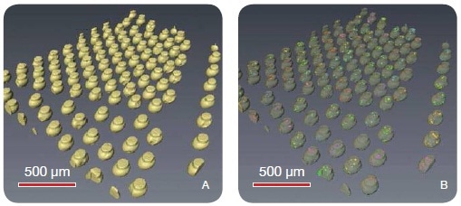
The results of the study are demonstrated in Figures 1 to 3. Figure 1A illustrates a 3D representation of the solder bumps, as isolated from the remaining part of the intact package. Segmentation and labeling of voids within each bump corresponding to the void volume are then performed as shown in Figure 1B.

Figure 1. (A) The solder bumps are visualized for feature localization and exterior analysis. (B) After void segmentation, the voids may be assigned a unique color (label) depending on the bump within which they are located, permitting bump-to-bump statistical void analysis.
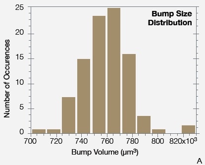
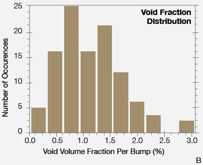
Besides imaging the voids within the bumps, the 3D data set facilitates void volume quantification, as shown in Figure 2, which demonstrates histograms of bump volume distribution (Figure 2A) and void volume fraction distributions (Figure 2B).


Figure 2. Statistical analysis of the results delivers quantities such as (A) bump volume and (B) void volume fraction distributions. The average bump volume is calculated to be 755000 µm3 and the average void volume fraction per bump is 1.14%.
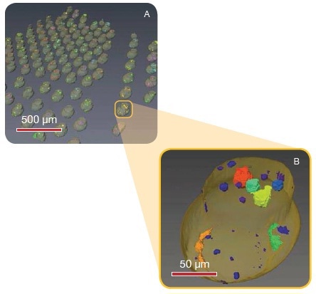
The segmentation of the large region of interest enables analysis of single bumps within the virtual volume, as demonstrated in Figure 3.

Figure 3. Using the Xradia VersaXRM-500 system, a large number of C4 bumps were imaged and independently analyzed for void sizes. Here, one bump has been virtually extracted from the region of interest and the voids labeled with different colors, corresponding to their 3D volume sizes (blue/purple = lowest volume, red = highest volume).
Conclusion
From the results, it is evident that the VersaXRM platform is able to deliver rapid and accurate non-destructive 3D metrology on solder bumps.

This information has been sourced, reviewed and adapted from materials provided by Xradia.
For more information on this source, please visit Xradia.