Jul 19 2009
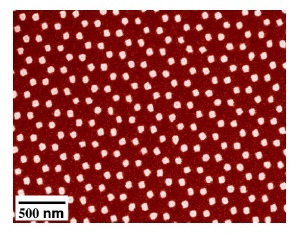
The first artificial graphene has been created at the NEST laboratory of the Italian Institute for the Physics of Matter (INFM-CNR) in Pisa. It is sculpted on the surface of a gallium-arsenide semiconductor, to which it grants the extraordinary properties of the original graphene. Published as a Rapid Communication on Phys.Rev.B, the research has been highlighted by the American Physical Society.

They envisioned it at the NEST laboratory in Pisa (a joint INFM-CNR and Scuola Normale Superiore di Pisa lab), and then they "sculpted" it like a work of art on the surface of a gallium-arsenide semiconductor. They named it "artificial graphene", the very first ever created, ready to raise the interests of both industry and research. This amazing "copy" promises to render available the incredible electronic qualities of graphene, and thus, it offers a way to overcome the closing physical limits that plague silicon. An exceptional result of Marco Gibertini, Achintya Singha, Marco Polini and Vittorio Pellegrini of INFM-CNR and Scuola Normale Superiore di Pisa, with the cooperation of Giovanni Vignale (University of Missouri), Aron Pinczuk (Columbia University) Loren Pfeiffer and Ken West (Alcatel-Lucent's Bell Labs).
Natural graphene is an interesting but elusive material, observed for the first time in 2004. It has a very peculiar structure, being composed of a single layer of carbon atoms (only one atom thick) arranged in a grid which resambles common chicken wire. This structure grants graphene its exciting electronic properties: over this two-dimensional carbon nanoworld, electrons move almost freely at very high speeds, acting like massless particles. For the electronic industry, this means more efficient devices that will be able to be built a lot smaller than what silicon allows. Such an innovation, however, is yet far away to come, because production of graphene with sizes and reproducibility needed by the semiconductor industry is not possible yet.
But, if currently-out-of-our-reach graphene offers so many desirable qualities, why not try to "trick" nature and "steal" its qualities creating a copy? An entriguing route, based on the idea that replicating graphene's structure on a different material might endow it with graphene's extraordinary properties. And this is exactly what that scientists at NEST tried with the help of gallium-arsenide semiconductors, objects widespread in the production of transistors and lasers. They carved a semiconductor with the help of an ion beam, creating a nanopattern on its surface that replicates the exact graphen's structure. And the idea proved to be a complete success: modified in this way, the nanosculptured semiconductor exhibits the properties of the famous material it imitates, thus becoming the very first artificial graphene. With an added advantage: the overall procedure does not rely on exotic equipments, but on tools and instruments that the nanofabrication industry already possesses and masters, meaning that the artificial graphene can already enable the development of high-mobility transistors and lasers.
"We are extremely happy" commented Vittorio Pellegrini and Marco Polini "to have been first in creating artificial graphene. This line of research has a great strategic importance, and for this reason very intense competition had sparkled between many research groups around the world. Being the first to create this material means in fact gaining a significant advantage in exploiting its extraordinary characteristics. And we believe that this 'artificial copy', already part of a semiconductor, may finally make graphene's properties available to be implemented in industrial projects and products."