Nov 3 2009
Novellus Systems (NASDAQ: NVLS) announced today that it has developed a new tungsten deposition process, called LRWxT, that can effectively reduce contact and line resistance at the 3Xnm technology node compared to conventional tungsten chemical vapor deposition (CVD-W) technology.
The new approach uses the company's ALTUS Max system for a unique deposition process sequence that results in highly conformal, large grain size films with lower tungsten bulk resistivity. The new process was developed and tested on device features provided by NEC Electronics, and the breakthrough was presented at this year's annual Advanced Metallization Conference in Baltimore.
As semiconductor manufacturing technology approaches 32nm design rules, memory and logic device manufacturers face challenges in scaling the resistivity of contacts, vias and bit line interconnects. The thinner tungsten films that are required to fill the smaller critical dimensions associated with 3Xnm devices have higher resistivity. This thin-film effect will continue to increase as these critical dimensions shrink at future nodes. To address the resistance scaling issue, Novellus developed the LRWxT tungsten deposition process that enables optimal feature fill while reducing the resistivity of the deposited bulk tungsten layer.
LRWxT employs the high productivity, multi-station sequential architecture of the ALTUS Max CVD-W system to deliver a unique, three-step deposition process. First, a <20Å thick nucleation layer is deposited using Novellus' proprietary PNLxT (Pulsed Nucleation Layer) technology. Next, a low-resistivity tungsten (LRWxT) treatment step is applied to promote growth of the low resistivity bulk film. Finally, an optimized CVD-W film is deposited for the bulk fill of nanometer-sized structures.
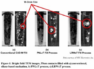
Figure 1 shows cross-sectional images of 55nm contact features filled with a) a process using conventional, silane-based nucleation, b) a PNLxT process, and c) the LRWxT process. The images show that the LRWxT filled features contain significantly larger tungsten grains as compared to the conventional process, and moderately larger grains than the PNLxT process. The large grain sizes and conformal fill are the key differentiating characteristics of the LRWxT process, and provide the mechanism for lower tungsten bulk resistivity.
"As semiconductor manufacturers advance to smaller technology nodes, minimizing the resistivity effects from device scaling is critical to improving electrical performance in logic and memory devices," said Dr. Patrick Lord, senior vice president for Novellus' Direct Metals, Surface Preparation, and Gapfill business units. "The ALTUS Max LRWxT process delivers industry-leading productivity to our customers while improving the speed and efficiency of their devices."