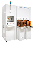
Rudolph Technologies, Inc. (NASDAQ: RTEC), a leading provider of process characterization equipment and software for wafer fabs and advanced packaging facilities, announced today that it has received multiple system orders from a major Asian foundry and an IDM (integrated device manufacturer) with fabrication facilities in the U.S. for its latest MetaPULSE-G opaque metrology tool. Shipments to fulfill these orders are scheduled for Q4 '10 through Q3 '11.
The MetaPULSE-G tool is Rudolph's latest addition to the MetaPULSE line of opaque thin film thickness measurement systems. A new 515nm ultra-fast laser light source provides significant improvements in signal to noise and measurement repeatability. In addition to these improvements, throughput gains for typical measurements of as much as 50 percent, to over 60 wafers per hour, have been realized. Combined, these features can offer improved performance on advanced copper interconnect structures as well as significant reductions in cost of ownership, due, in large part, to higher throughput and lower cost of consumables.
 MetaPULSE-G System
"Interconnect metrology is becoming more challenging as our customers move to the 32nm process node and below. Thinner interconnect layers are driving needed improvements in film stack measurement precision and repeatability," said Tim Kryman, Rudolph's metrology business product manager. "In addition, pattern-dependent deposition characteristics exhibited in today's advanced processes are pressing IDMs and foundries to move from monitor wafer and scribe line measurements to on product metrology. The MetaPULSE-G system's unique laser source and improved signal detection are providing our customers a metrology solution with the required precision and repeatability at throughputs 1.5 to 2 times greater than competitive technologies. Similar to other systems in the MetaPULSE product line, the MetaPULSE-G tool also offers a small spot size which allows measurements to be made on product where actual device performance is determined. This all adds up to a unique combination of advanced capability and low cost of ownership which is driving customer acceptance."
Rudolph's MetaPULSE tools, the industry standard for opaque film metrology, use a laser-generated sonar pulse to measure the thickness and other properties of the material layers used to build a semiconductor device. In contrast to X-ray-based technologies, the small spot size of the MetaPULSE tools permits measurements directly on product wafers. Unlike optical critical dimension (OCD) technologies, MetaPULSE tools allow fast, easy creation of new recipes and do not require special structures like solid copper pads under measured structures.