GaN based epitaxy on silicon (Si) is very challenging because of the thermal mismatch between GaN and Si, which causes extreme tensile stress after cooling. For such applications LayTec's EpiCurveTT is the tool of choice for a precise in-situ strain engineering. Prof. Alois Krost and his team at the Ottovon- Guericke University (OvG) in Magdeburg, Germany, applied the tool to develop a new strain engineering method by using germanium (Ge) as n-dopant instead of Si.
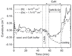
The figure shows curvature measurement on two differently doped GaN/Si samples. The downward slope after the LT-AlN interlayer growth indicates compressive stress. With the addition of Si as dopant, the slope inverts (solid line), the Si doping causes tensile stress and during cooling the sample cracks. In the case of Ge doping, however, the curvature slope remains unchanged (dashed line) and the sample remains crack-free.
 In-situ curvature measurements with EpiCurve®TT of GaN/Si with Si
doping (solid line) and Ge doping (dashed line).
Photoluminescence spectra of the Ge doped GaN shows a doubled luminescence intensitiy compared with the Si doping. This proves good material quality of the approx. 1.6 ìm thick GaN structure.
According to Armin Dadgar of OvG University, "the idea to dope GaN-on-silicon with an alternative dopant is quite old. But now, with strain control and engineering with mixed dopants, EpiCurveTT gives a new impulse for GaN/Si device applications."