James Tour, a lab chemist at the Rice University, has published two research papers that describe the novel production processes of superior-quality bilayer graphene on a large scale onto various insulating substrates directly.
‘Growth of Bilayer Graphene on Insulating Substrates’ and ‘Direct Growth of Bilayer Graphene on SiO2 Substrates by Carbon Diffusion Through Nickel,’ are the titles of the two papers, which describe the method to develop bilayer graphene on a functional substrate by first making it to diffuse into a nickel layer.
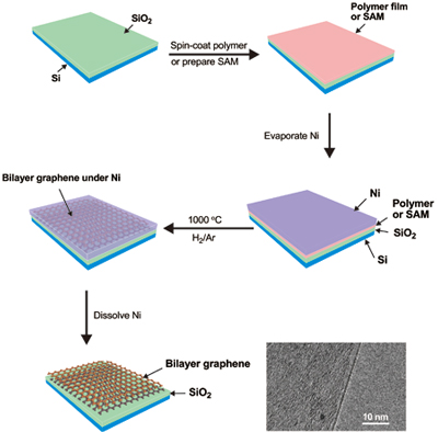
 This graphic shows the process of creating bilayer graphene on an insulating substrate, skipping the need to transfer graphene from a metal catalyst. The final image, captured with an electron microscope, clearly shows two layers of graphene produced via the process. Credit: Tour Lab/Rice University
Tour stated that the novel processes’ ability to develop bilayer graphene straightaway onto a insulating substrate can allow electronics device producers to eliminate the troublesome process of stacking graphene sheets on one another in the building of transistors. The novel methods are based on the carbon atom solubility in heated nickel.
In the first study, a nickel coat is evaporated onto silicon dioxide and a polymer film is placed on top. The polymer is diffused into the metal when the sandwich is heated to 1,000° C in a stream of hydrogen and argon gases. When the sandwich is cooled, graphene is produced on the silicon dioxide and the nickel surfaces. Upon etching away of the nickel and incidental graphene that was created on top, bilayer graphene remained on the silicon dioxide substrate. The research was supported by the Air Force Office of Scientific Research, Lockheed Martin and Office of Naval Research MURI program.
In the second study, the researchers sandwiched a polymer layer between the silicon dioxide and nickel. When low pressure and high temperature is applied, bilayer graphene is formed between nickel and silicon dioxide. The researchers also demonstrated that bilayer graphene can also be formed on sapphire, silicon nitride and hexagonal boron nitride. The research was supported by M-I SWACO, the Air Force Office of Scientific Research, the Air Force Research Laboratory via United Technology Corp. and the Office of Naval Research MURI program.