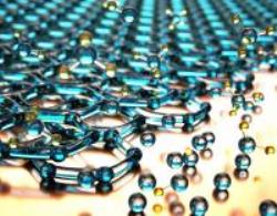
In a research led by Kaustav Banerjee, University of California-Santa Barbara’s (UCSB) Electrical and Computer Engineering professor and Director of Nanoelectronics Research Lab, a team of scientists have developed a new method of growing graphene in a restricted manner to make it suitable for large scale use in electronic applications.
 Graphene
For graphene to be used effectively in electronic applications, it has to be developed in large sheets. Though graphene is stronger than diamond and displays superior conductivity, developing it for the purpose of large scale production has been difficult.
However, this research, which is funded by the National Science Foundation and carried out by UCSB’s Materials Research Laboratory and California NanoSystems Institute, has used a method called Low Pressure Chemical Vapour Deposition (LPCVD), under which the hydrocarbon gas, methane was disintegrated at a particular temperature. As a result graphene was formed in uniform layers on a copper substrate that was treated earlier. Scientists were also able to create graphene with single and two layers and maximized the quality and uniformity of graphene by a set of techniques. Graphene created in this manner had an average value of 4000 cm²/V.s and maximum peak value 5500 cm²/V.s, which is much higher than the values of silicon. The group led by Kaustav Banerjee is focussed on developing nanoelectronics and undertakes research of designing of devices, circuit and exploring it and synthesis of material.