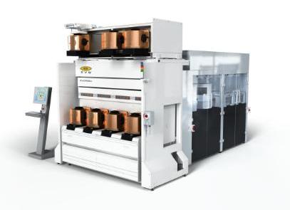
EV Group, a provider of lithography and wafer bonding devices for the semiconductor, nanotechnology and MEMS industries, has expanded its portfolio of GEMINI FB fusion wafer bonder with the launch of a novel platform called the XT Frame that improves tool functionality and process throughout for most of its existing high-volume products.
 EV Group's new XT Frame platform (Credit:PRNewsFoto/EV Group)
EV Group’s XT Frame platform, exclusively developed to meet the needs of mass-producing customers, is capable of housing a maximum of nine process modules, which is two times higher than that of the company’s earlier optimal processing functionality for improved process throughput. Moreover, it provides more options to customers for accommodating various process modules on one tool platform.
The XT Frame architecture offers an ultrafast handling tool, a device front-end module, four front opening unified pod (FOUP) load ports and sufficient module spaces for performing simultaneous processing of numerous wafers. These features along with a material buffer as a local FOUP storage system delivers nonstop mode of operation with high efficiency. The platform meets additional customer needs, including compact size, enhanced serviceability, easy upgradeability and more process options by allowing the combination of various process modules on single equipment.
EV Group’s XT Frame is specially designed for sophisticated three-dimensional and packaging interlink applications with through-silicon vias. In this field, the new architecture is capable of improving the performance of the company’s standard temporary thin wafer and bonding or debonding processing systems. In order to demonstrate the platform’s capabilities, the company has developed its EVG850TB/DB system on it. The EVG850TB/DB system is also capable of accommodating the company’s Edge Zone Debond and Edge Zone Release modules to complement the ZoneBOND technology.