A new manufacturing method to produce novel structures made of various semiconductors has been developed by scientists from CSEM, ETH Zurich, Università di Milano-Bicocca and Politecnico di Milano. The semiconductor structures can be produced in any thickness on silicon substrates, which are cheap and found in abundance.
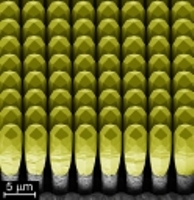 Perspective scanning electron micrograph of an array of ~8 micrometers tall, facetted Germanium crystals grown on Silicon pillars.
The novel structures comprise a series of individual crystals that are separated by thin nanometer gaps. The production of these structures involve a few steps. At first, a silicon wafer is fabricated using photolithography method and is followed by etching of the wafer into a structure that resembles a chocolate bar. The next step is growing the structure over the substrate under appropriate conditions, which ensure a smallest separation between the crystals. This results in three-dimensional semiconductor structures. The method, developed by ETH Zurich team, has produced defect-free germanium structures over the silicon wafers and a height of 50 µm has been achieved.
The method prevents the formation of crystal defects that are usually present in atomic layers. In addition, it considerably reduces the bending of substrates over temperature changes, which is mainly caused by uneven thermal coefficients of expansion of dissimilar materials. Another important benefit of the process is the absence of critical layer cracking, resulting from thermal strains.
The semiconductor structures have innovative applications in a wide range of fields, including medical, solar energy and power electronics. One important application is the X-ray imaging detectors, which require thick germanium absorbers. The new approach helps to considerably minimize doses essential for X-ray imaging in the medical sector. The method is also suitable for multiple-junction solar photovoltaic cells used for space and concentrator applications. It substitutes heavy, delicate and costly germanium substrates with light-weight and cheap ones. Thus, the approach offers significant reduction in weight and cost.