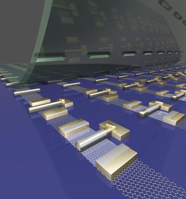
Graphene, a one-atom-thick graphitic carbon layer, shows promise to be used as a transistor that may help develop faster and smaller consumer electronic devices.
 Self-aligned graphene transistor
However, reducing dimensions of electronics and graphene’s novel properties make the nanomaterial difficult to produce on a larger scale. The deployment of traditional fabrication methods to produce high-performance graphene often causes damage to the nanomaterial’s lattice structure and affects its performance, leading to issues such as serial resistance and parasitic capacitance.
To overcome these challenges, scientists from the UCLA Department of Chemistry and Biochemistry, the UCLA Henry Samueli School of Engineering and Applied Science’s department of materials science and engineering, and UCLA’s California NanoSystems Institute have devised a proven scalable technique to fabricate self-aligned graphene transistors featuring transferred gate stacks.
The new technique involves traditional lithography, etching and deposition processes on a sacrificial substrate prior to integration with large-area graphene by a physical transferring process, thus enabling it to handle the issues of traditional fabrication. With the combination of a self-aligned device structure and a damage-free transfer process, the new technique has made it possible to fabricate high-speed, self-aligned graphene transistors with over 400 GHz of cutoff frequency, the highest value so far.
This unique scalable technique holds potential for future use of graphene-based electronic devices in ultra–high-frequency circuits.
The U.S. Office of Naval Research, the National Institutes of Health, and the National Science Foundation supported the work. The study results have been reported in the journal, Proceedings of the National Academy of Sciences.