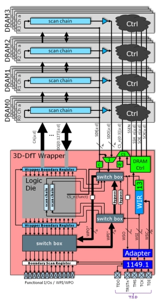
At the European 3D TSV Summit in Grenoble, France on January 22-23, 2013, imec, a world-leading nano-electronics research institute, today announced that together with Cadence Design Systems they have developed, implemented and validated an automated 3D Design-for-Test (DFT) solution to test logic-memory interconnects in DRAM-on-logic stacks. The solution, based on Cadence® Encounter® Test technology, was verified on an industrial test chip containing a logic die and a JEDEC-compliant Wide-I/O Mobile DRAM.
 Imec’s 3D wrapper extension for Wide-I/O DRAM
Memory-on-logic 3D stacks offer the possibility of heterogeneous integration with dense low-power inter-die interconnects. Hence, they are amongst the first 3D products that will come on the market, enabling next-generation high-performance low-power mobile applications. Recently, JEDEC has released a standard (JESD-229) for stackable Wide-I/O mobile dynamic random access memories (DRAMs) specifying the logic-memory interface. Unlike many previous DRAMs, the standard contains boundary scan features to facilitate interconnect testing. Imec and Cadence now present a design-for-test (DFT) architecture and corresponding automatic test pattern generation (ATPG) approach. It is an extension of their previously announced logic-on-logic 3D DFT architecture and it supports post-bond testing of the interconnects between the logic die and the DRAM stacked on top of it.
The solution implemented by Cadence and imec includes the generation of DRAM test control signals in the logic die and the inclusion of the DRAM boundary scan registers in the serial and parallel test access mechanisms (TAMs) of the 3D test architecture. The automated design for test solution has been validated on an industrial test chip. The design of the test chip is an interposer-based 3D stacked IC which includes a silicon interposer base die, a 94mm2 logic system-on-chip in 40nm technology, and a single Wide-I/O DRAM rank. The validation results show that the silicon area of the additional DFT wrapper is negligible compared to the total logic die size (<0.03%). Moreover, the test pattern generation was very efficient (tens of patterns, generated in only a few seconds) and effective (100% coverage of the targeted faults). All 3D-DFT logic in the logic die was automatically inserted with Cadence Encounter RTL Compiler while the Interconnect test patterns were generated with Encounter Test ATPG.
“This 3D memory-on-logic DFT solution is another big step forward toward market introduction of 3D-stacked IC for next-generation high–performance, low-power mobile applications,” said Bassilios Petrakis, product marketing director for the Encounter Test product family at Cadence. “Our collaboration with imec has enabled the creation of an industry-leading solution that enhances efficiencies of 3D-IC design for our customers.”
“Teaming up with Cadence enables us to automate the insertion of our DFT circuitry in a given design, and to automate the interconnect test pattern generation. Such automated flows make our technology valuable for the industry. We are confident that we can also handle the DFT features that start to emerge in other 3D memory standards,” said Erik Jan Marinissen, Principal Scientist at imec.
Part of the work has been performed in the project ESiP, which is co-funded by the ENIAC Joint Undertaking.