Feb 5 2014
Working on the cutting edge of a newly emerging area of solar-cell research, UCLA engineers have invented a new process for manufacturing highly efficient photovoltaic materials that shows promise for low-cost industrial production.
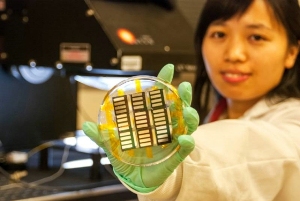
 UCLA's Huanping Zhou displays perovskite solar cells.
The new process uses so-called perovskite materials, which in the past few years have significantly advanced scientists' efforts to create the next generation of solar cells.
The term "perovskite" is a reference to a mineral called perovskite, which was first discovered in Russia in the 1830s. Perovskite solar cells are not made from the mineral itself, but they mimic its crystalline structure, which has proven to be particularly efficient for harvesting light to generate electricity.
Technological advances have enabled scientists to create perovskite crystals with different compositions that are suited to perform different functions. The UCLA team's research focused on perovskite crystals made from a hybrid of inorganic and organic materials — methyl ammonium halide and lead halide, respectively — which are then made into a thin film that is sandwiched between two electrodes.
Led by Yang Yang, the Carol and Lawrence E. Tannas Jr. Professor of Engineering at the UCLA Henry Samueli School of Engineering and Applied Science, the UCLA researchers devised a way to produce solar cells using those materials more efficiently and cost-effectively than the current standard methods.
Until now, engineers have typically created the perovskite film using one of two processes: Either a solution of the organic and inorganic materials is used to create the film or the two components are thermally evaporated together inside a vacuum chamber. While each technique has been successful in research labs, both are challenging for large-scale industrial production. The wet process results in decreased film quality, and the vacuum process requires expensive equipment and uses a great deal of energy.
The UCLA team's new approach is a vapor-assisted solution process that efficiently produces perovskite solar cells without the flaws associated with the other techniques.
The vapor-assisted process involves coating a substrate with the inorganic component and then treating it in a steam bath of organic molecules at about 150 degrees Celsius. The organic material infiltrates the inorganic matter and forms a compact perovskite film that is significantly more uniform than the films produced by the wet technique.
In a few test runs, the technique has produced solar cells with a highly efficient power conversion rate of more than 12 percent — a rate comparable to or better than that of the amorphous silicon solar cell — and the UCLA researchers are working toward improving that performance. Equally important, the process, which in the lab was used to develop postage stamp–sized solar cells, appears to have the potential to be scaled up to develop larger cells for use in commercial applications.
Research describing the new process was published online Dec. 20 by the peer-reviewed Journal of the American Chemical Society, and in the journal's Jan. 15 print edition.
"Perovskite cells are one of today's most promising solar technologies," said Yang, who also is a member of the UCLA California NanoSystems Institute. "Over the last year, the gains of perovskite solar cells in efficiency of converting sunlight to electricity far outpace the incremental gains of other solar materials. Now, we have identified a process by which this material can be inexpensively and easily processed."
Yang said there are still technical challenges to overcome, including the material's propensity to absorb moisture when not properly encapsulated, which degrades its device performance. In addition, the lead used in the perovskite production poses environmental concerns.
Huanping Zhou, a postdoctoral researcher in UCLA's materials science and engineering department and UCLA's California NanoSystems Institute, and the paper's corresponding author, said the new technique works efficiently because the organic materials' melting point is low, and the organic and inorganic components react with each other rapidly. "As a result, the organic material can quickly intercalate into the inorganic material and become a consistent layer of perovskite that is high quality, inexpensive and easy to manufacture," she said.
Zhou said the process could eventually also be adapted to use organic-inorganic hybrid materials for producing transistors, light-emitting diodes and other devices.
Qi Chen, a postdoctoral researcher in UCLA's materials science and engineering department and CNSI, is the lead author of the research. Other authors include Ziruo Hong and Gang Li, research engineers in UCLA materials science and engineering; postdoctoral researcher Yongsheng Liu; and graduate students Song Luo, Hsin-Sheng Duan and Hsin-Hua Wang, all of UCLA materials science and engineering and CNSI.
The research was supported by the National Science Foundation, the Air Force Office of Scientific Research and UCLA.