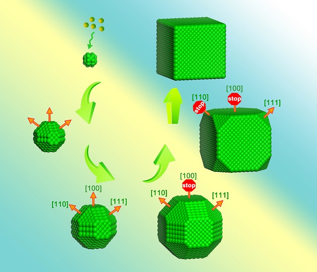
The geometric shape of the crystal can be controlled by ascertaining how faces or facets form on a nanocrystal. This in turn is crucial in determining the electronic and chemical properties of the crystal.
This research was lead by Haimei Zheng, a scientist in the Materials Sciences Division of Berkeley Lab. The research team established that at the molecular level, the nanocrystals’ geometric shape while synthesizing in solution is controlled by the variation in ligand mobility across different facet surfaces.

Image Caption - Berkeley Lab researchers found that differences in ligand mobility during crystallization cause the low index facets – {100}, {110} and {111} – to stop growing at different times, resulting in the crystal’s final cubic shape. (Image courtesy of Haimei Zheng group)
Haimei explains that the shape of the growing nanocrystal can be controlled by selecting ligands that attach to the facets in a specific pattern. This will enable innovative nanomaterial design for sophisticated applications such as solar conversion catalysts, energy storage and bio-imaging nanostructures.
The lead author of the paper detailing this research published in Science, is Hong-Gang Liao and the corresponding author is Zheng. The co-authors of the paper are Huolin Xin, Danylo Zherebetskyy, Peter Ercius, Ming Pan, Hans Elmlund, Cory Czarnik, and Lin-Wang Wang.
TEM - platinum nanocube
The researchers grew the nanocubes in a thin liquid layer packed between two membranes of silicon nitride while working with a highly effective industrial catalyst, platinum. This micro liquid cell is capable of retaining the liquid in the high vacuum atmosphere of a TEM for an extended time period allowing in situ observations of the growth trajectories of single nanoparticles.
Zheng’s team were able to use many of the TEMs at the National Center for Electron Microscopy, Berkeley Lab including the most powerful TEM worldwide, the TEAM 0.5 instrument. Furthermore, they used the K12-IS camera from Gatan, which enables the capture of electron images onto a CMOS sensor directly at 400 fps with 2K by 2K resolution. The DOE Office of Science supported the research.
For more information about the research of Haimei Zheng go here
For more information on Berkeley Lab’s National Center for Electron Microscopy go here
References