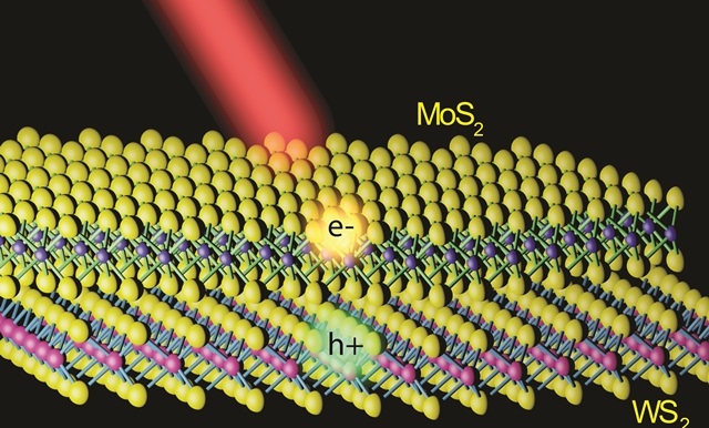
 Illustration of an MoS2/WS2 heterostructure with an MoS2 monolayer lying on top of a WS2 monolayer. Electrons and holes created by light are shown to separate into different layers. (Image courtesy of Feng Wang group)
An international research team led by a Berkeley Lab scientist has reported ultrafast charge transfer time of below 50 femtoseconds in photo-excited MX2 heterostructures. This research has established that MX2 materials, which are 2D semiconductors, have excellent optical and electrical properties and are highly promising for potential optoelectronic, photonic and also photovoltaic applications.
This research has been published in Nature Nanotechnology. Feng Wang, condensed matter physicist with the Material Science Division of Berkeley Lab and the Physics Department of the University of California (UC) Berkeley, is the corresponding author of the paper.
The paper is titled “Ultrafast charge transfer in atomically thin MoS2/WS2 heterostructures” and the co-authors are Jonghwan Kim, Xiaoping Hong, Yu Zhang, Su-Fei Shi, Chenhao Jin, Sefaattin Tongay, Yinghui Sun, Yanfeng Zhang and Junqiao Wu.
MX2 monolayers include a single transition metal atom layer such as tungsten or molybdenum, sandwiched between two chalcogen atom layers such as sulfur. The van der Waals force binds the resulting heterostructure. These 2D semiconductors are very similar to graphene in terms of the hexagonal honeycomb structure they possess and excellent electrical conductance.
However, the MX2 materials have natural energy band gaps unlike graphene. They can hence be used in electronic devices and transistors as their electrical conductance can be turned on and off.
Wang stated that MX2 materials have excellent optical absorption properties and, in comparison with organic photovoltaic materials, have superior electrical transport properties and a crystalline structure.
He added that the team desires to use external electrical fields to control the charge transfer process in order to use MX2 heterostructures in photovoltaic devices.
The DOE Office of Science supported this research work with an Early Career Research Award through UC Berkeley, and also the work was supported by Chinese funding agencies through the Beijing Peking University.
This news come not long after the Lawrence Berkeley National Laboratory was used to verify the three dimensional structure of a gold nanoparticle at atomic resolution and the recording of physical mechanisms that control the evolution of facets on platinum nanocube surfaces.