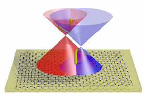
A team of scientists from Manchester, Nottingham and Lancaster Universities, and associates from Russia, Japan and Seoul, have shown that perfect crystals for next generation transistors could be created by joining 2-D materials in a stack. The research team was led by Nobel laureate Sir Kostya Novoselov of the University of Manchester.
 Tunneling transistors could open up new ranges of electronic devices
In 2004, during research on isolation of graphene, a family of 2-D materials was discovered. White graphene or Hexagonal boron nitride (hBN) was one among these materials.
In previous studies, researchers at the University of Manchester had shown that combination of 2-D materials in heterostructure stacks could help develop materials for industrial applications.
In the present research, the team demonstrated that by accurately controlling crystalline layer orientation within the heterostructures, their electronic behavior could be altered by a great degree.
The research team found that conservation of momentum and electron energy occurred when two graphene electrodes were aligned carefully and separated by white graphene. This discovery could lead to development of electronics, photovoltaic sensors and ultra-high frequency devices.
A University of Manchester and Nottingham joint academic, Professor Laurence Eaves, stated that the present study arose from electrons’ quantum wave nature and the classical laws of motion, which would allow them to go through barriers.
This research arises from a beautiful combination of classical laws of motion and the quantum wave nature of electrons, which enables them to flow through barriers. We are optimistic that further improvements to the device design will lead to applications in high-frequency electronics.
Professor Laurence Eaves, a joint academic from the Universities of Manchester and Nottingham
Vladimir Falko, a Professor at the Lancaster University, commented that the observation by researchers of negative differential conductance and tunneling in devices that were produced from hBN and multilayers of graphene, showed the system’s potential for electronics devices and applications. This present study used mechanical transfer technique. However, material growers must find methods using growth techniques for making multilayer systems.
This study has been published in Nature Nanotechnology.
References