Nov 14 2014
North Carolina University researchers have devised a new technique of transferring one-atom-thick semiconductor films to arbitrary substrates, which may help realize photonic devices or flexible computing.
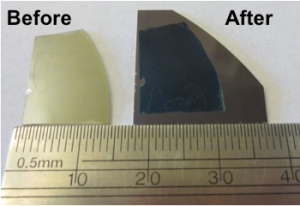
 Image of the thin film on the original growth substrate (left) and after being transferred (right). Photo credit: Linyou Cao.
NC State assistant professor of materials science and engineering, Dr Linyou Cao initially developed the one-atom-thick molybdenum sulfide(MoS2) thin film. MoS2 is a low-cost semiconductor material having optical and electronic properties similar to others being used in the semiconductor industry.
The final aim is to create highly flexible devices using these one-atom-thick semiconducting films, however that goal can be accomplished only by transferring the thin films to a flexible substrate. It is not feasible to create the thin film on the substrate itself since such high temperatures cannot be endured by flexible substrates.
The one-atom-thick and 5cm diameter MoS2 films created by Cao’s team needed to be moved without cracking or wrinkling it, which was a great challenge.
Presently available techniques include chemical etching but that may contaminate or damage the film. The method adopted by Cao’s team involved the use of a tissue, water at room temperature and a pair of tweezers for transferring the thin film onto the substrate.
Hydrophobic MoS2 repels water; however the hydrophilic sapphire substrate on which the thin film is grown, attracts water. The novel transfer technique involves the application of a water drop to the thin film, after which a scalpel or tweezers is used to make the water infiltrate between the sapphire and MoS2.
Moving Atomically Thin Films
Once it starts penetrating, the water forces itself into the gap causing the thin film to float on top. A tissue was used by the researchers for drying the water and then the thin film was transferred onto the flexible substrate using tweezers. The complete process takes two minutes, however chemical etching takes several hours.
This new transfer technique gets us one step closer to using MoS2 to create flexible computers. We are currently in the process of developing devices that use this technology.
Dr Linyou Cao
The water weakens the bond between the thin film and the substrate, however it is essential to dry the water before the film is moved or else, capillary action may cause folding or buckling of the film while it is picked. According to the researchers, the new transfer method has helped them draw nearer to the dream of using MoS2 to design flexible computers.
References