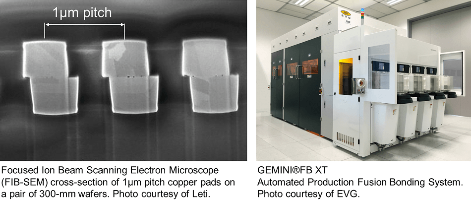
EV Group (EVG), a leading supplier of wafer bonding and lithography equipment for the MEMS, nanotechnology and semiconductor markets, and Leti, an institute of CEA Tech, today announced the world’s first successful 300-mm wafer-to-wafer direct hybrid bonding with pitch dimension connections as small as 1µm (micron). This breakthrough also achieved copper pads as small as 500nm.
The copper/oxide hybrid bonding process, a key enabler for 3D high-density IC applications, was demonstrated in Leti’s cleanrooms using EVG’s fully automated GEMINI®FB XT fusion wafer bonding system. This result was obtained in the framework of the program IRT Nanoelec headed by Leti. EVG joined the institute’s 3D Integration Consortium in February 2016.

Wafer Bonding an Enabling Process for 3D Device Stacking
Vertical stacking of semiconductor devices has become an increasingly viable approach to enabling continuous improvements in device density and performance. Wafer-to-wafer bonding is an essential process step to enable 3D stacked devices. However, tight alignment and overlay accuracy between the wafers is required to achieve good electrical contact between the interconnected device on the bonded wafers, as well as to minimize the interconnect area at the bond interface so that more space can be made available on the wafer for producing devices. The constant reduction in pitches that are needed to support component roadmaps is fueling tighter wafer-to-wafer bonding specifications with each new product generation.
Demonstration Results
In the Leti demonstration, the top and bottom 300-mm wafers were directly bonded in the GEMINI FB XT automated production fusion bonding system, which incorporates EVG’s proprietary SmartView®NT face-to-face aligner and an alignment verification module to enable in-situ post-bond IR alignment measurement. The system achieved overlay alignment accuracy to within 195nm (3-sigma) overall, with mean alignment results well centered below 15nm. Post-bake acoustic microscopy scans of the full 300-mm bonded wafer stack as well as specific dies confirmed a defect-free bonding interface for pitches ranging from 1µm to 4µm with optimum copper density.
To our knowledge, this is the first reported demonstration of sub-1.5µm pitch copper hybrid bonding feasibility, this latest demonstration represents a real breakthrough and important step forward in enabling the achievement and eventual commercialization of high-density 3D chip stacking.
Frank Fournel, head of bonding process engineering at Leti.
This demonstration is summarized in a paper co-authored by Leti, titled “1 µm Pitch Direct Hybrid Bonding with <300nm Wafer-to-wafer Overlay Accuracy,” which was presented at the 2017 IEEE S3S Conference.
3D integration holds the promise for increased device density and bandwidth as well as lower power consumption for a variety of applications, from next-generation CMOS image sensors and MEMS to high-performance computing, as a leader in 3D integration research and development, Leti has been at the forefront in moving this critical technology toward industry adoption and commercialization. EVG shares that vision, and we are pleased to have played a role in supporting Leti’s latest achievement in 3D integration.
Markus Wimplinger, corporate technology development and IP director at EV Group.
Leveraging EVG’s high-throughput XT Frame platform and an equipment front-end module (EFEM), the GEMINI FB XT automated production fusion bonding system is optimized for ultra-high throughput and productivity. The SmartView NT aligner integrated into the system provides industry-leading wafer-to-wafer overlay alignment accuracy (sub-200nm, 3-sigma). In addition, the GEMINI FB XT can accommodate up to six pre- and post-processing modules for surface preparation, conditioning and metrology steps such as wafer cleaning, plasma activation alignment verification, debonding (allowing pre-bonded wafers to be separated automatically and re-processed if necessary) and thermo-compression bonding.
EVG will showcase the GEMINI FB XT at the SEMICON Europa exhibition being held November 14-17 at the Messe München in Munich, Germany. Attendees interested in learning more about the product, as well as EVG’s full suite of wafer bonding and lithography solutions, are invited to visit the company’s booth
#B1-1424.