Dec 5 2017
A team of scientists from Japan has declared that they have been the first to quantif the effects of three electron-scattering mechanisms for ascertaining the resistance of silicon carbide (SiC) power semiconductor devices used in power semiconductor modules.
The university-industry group comprising scientists from the University of Tokyo and Mitsubishi Electric Corporation has discovered that resistance below the SiC interface can be minimized by nearly two-thirds by preventing electron scattering by the charges. Their findings are anticipated to assist in minimizing the consumption of energy in electric power equipment by reducing the resistance of SiC power semiconductors.
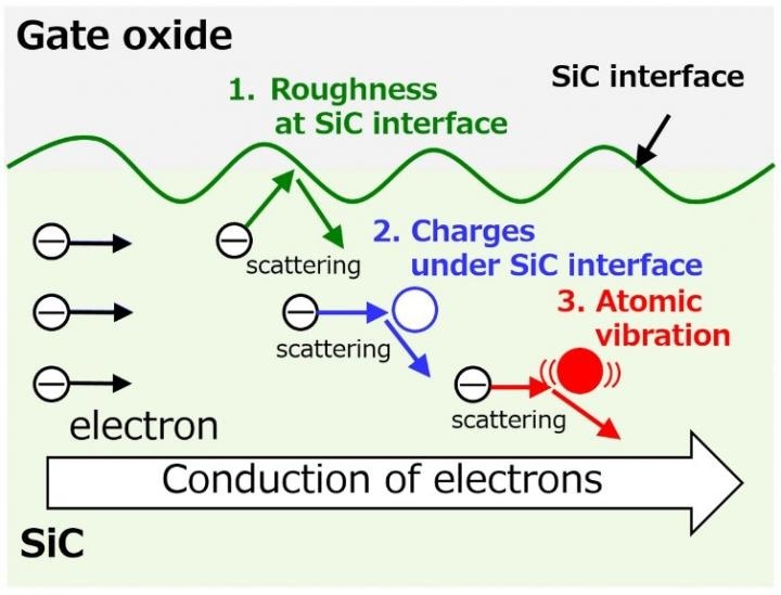
 Electron scattering under the silicon carbide (SiC) interface is limited by three factors: roughness of the SiC interface, charges under the SiC interface and atomic vibration. CREDIT: 2017 Mitsubishi Electric Corporation.
A combination of reduced size and increased efficiency is needed for electric power equipment applied in industrial machinery, home electronics, trains, and other devices. Mitsubishi Electric, a leading Japanese manufacturer of electronics and electrical equipment, has been increasing the application of SiC devices for power semiconductor modules, important components used in electric power equipment. When compared to traditional silicon power devices, SiC power devices exhibit lower resistance. Hence to reduce their resistance further, the properties of the resistance below the SiC interface have to be understood in-depth.
“Until now, however, it had been difficult to measure separately resistance-limiting factors that determine electron scattering,” stated Satoshi Yamakawa, senior manager of the SiC Device Development Center at Mitsubishi Electric’s Advanced Technology R&D Center.
Electron scattering targeted at atomic vibration was evaluated by applying technology from the University of Tokyo. The effect of atomic vibration and charges on electron scattering below the SiC interface was observed to be more powerful during the investigation of fabricated devices by Mitsubishi Electric. While researchers have identified that electron scattering below the SiC interface is restricted by three factors—the charges under the SiC interface, the roughness of the SiC interface, and the atomic vibration—the role played by each factor was unpredictable. The team fabricated a planar-type SiC metal-oxide-semiconductor field-effect transistor, or SiC-MOSFET, in which electrons are directed away from the SiC interface to nearly several nanometers, to validate the effect of the charges.
“We were able to confirm at an unprecedented level that the roughness of the SiC interface has little effect while charges under the SiC interface and atomic vibration are dominant factors,” stated Koji Kita, an associate professor at the University of Tokyo’s Graduate School of Engineering and one of the lead researchers of the study.
For comparison, the researchers used a previous planar-type SiC-MOSFET device and minimized the resistance by two-thirds because of avoiding electron scattering. They accomplished this by directing the electrons away from the charges below the SiC interface. The earlier planar-type device has an interface structure identical to that of the SiC-MOSFET developed by the electronics maker.
For the investigation, Mitsubishi Electric performed the designing, fabrication, and investigation of the resistance-limiting factors, whereas the University of Tokyo carried out the evaluation of electron-scattering factors.
“Going forward, we will continue refining the design and specifications of our SiC MOSFET to further lower the resistance of SiC power devices,” stated Yamakawa from Mitsubishi Electric.
This scientific accomplishment was declared on December 4, 2017, at the 63rd International Electron Devices Meeting (IEDM) in San Francisco, California.