Jan 11 2019
Transistors are prerequisites for devices involving current flow, and they are an obligatory component of almost all electronic switches. Transistors are used in the field of power electronics to switch large currents. Yet, one of its undesirable effects is that the components heat up, consequently leading to energy loss.
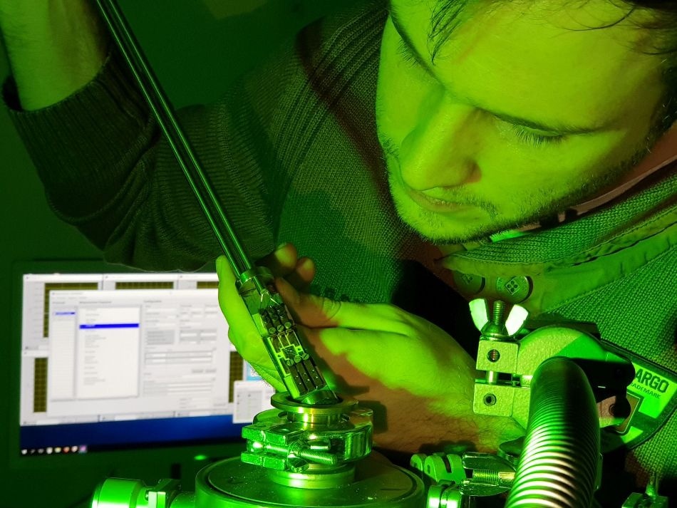 Physicist Martin Hauck fits a silicon carbide transistor into the measuring apparatus: researchers at FAU have discovered a method for finding defects at the interfaces of switches. (Image credit: FAU/Michael Krieger, Martin Hauck)
This can be dealt with by using energy-efficient transistors, potentially making substantial savings. Scientists at Friedrich-Alexander-Universität Erlangen-Nürnberg (FAU) have created a simple but accurate technique for identifying defects in the most recent generation of silicon carbide transistors. This will accelerate the process of building more energy-efficient transistors in the future. The outcomes of the study have now been reported in the eminent journal Communications Physics.
One way to save energy in the current highly technological world is to boost the efficiency of power electronic devices. This is because these are the components that make sure that power from photovoltaic or wind power stations is supplied to the grid, current from the overhead line is supplied to the traction units of trains, and energy is transferred from batteries to the engine in electric and hybrid vehicles. Meanwhile, it is necessary for these components to preferably use as little electricity as possible. Else, there will be an undesirable generation of heat, leading to the need for additional complex cooling systems and ensuing wastage of energy.
Components made using silicon, the conventional semiconductor material, reach their limits at this point based on their intrinsic material properties. However, there exists a considerably more appropriate alternative: silicon carbide (SiC)—a compound made of silicon and carbon. Its properties are obvious and self-revealed: it works even at high temperatures, endures high voltages, is chemically robust, and can work at high switching frequencies, thereby enabling even better energy efficiency. For many years, SiC components have been successfully used.
Investigating charge trapping
Power electronic switches developed using silicon carbide, also called field-effect transistors or MOSFETs, work based on the interface between the SiC and a very thin layer of silicon oxide deposited or developed on it. However, this interface is the one that poses a high difficulty for researchers: at the time of fabrication, unwanted defects are formed at the interface, trapping charge carriers and decreasing the electrical current in the device. Hence, analysis of these defects is of utmost significance if the potential offered by the material is to be completely exploited.
Pattern discovered
Traditional measurement methods typically developed by bearing silicon MOSFET devices in mind simply overlook the occurrence of such defects. Although there exist various other measurement methods, they are more time-consuming and complicated, and are either inappropriate for use on a large scale or are simply not ideal for being used on finished components. Hence, scientists at the Chair of Applied Physics at FAU made a decision to concentrate on discovering innovative, optimized techniques for probing interface defects—and they were successful.
It was observed by the researchers that the interface defects always followed the same pattern.
We translated this pattern into a mathematical formula. Using the formula gives us a clever way of taking interface defects into account in our calculations. This doesn’t only give us very precise values for typical device parameters like electron mobility or threshold voltage, it also lets us determine the distribution and density of interface defects almost on the side.
Martin Hauck, Physicist, Doctoral Candidate, Friedrich-Alexander-Universität Erlangen-Nürnberg.
The extremely simple technique was found to be highly accurate during experiments performed using transistors specifically designed for the purpose by the industrial partners of the researchers: Infineon Technologies Austria AG and its subsidiary Kompetenzzentrum für Automobil- & Industrie-Elektronik GmbH. Improved and shorter innovation cycles can be ensured by a deeper analysis of the inner core of the field-effect transistors. This technique can be used to quickly, accurately, and simply assess the processes intended to reduce defects. It will also enable rapid development of innovative, more energy-saving power electronics.