This week, at the 2019 Symposia on VLSI Technology and Circuits (June 9-14, 2019), imec, a world-leading research and innovation hub in nanoelectronics and digital technologies, demonstrates field-free switching operation of spin-orbit torque MRAM (SOT-MRAM) devices – eliminating the need for an external magnetic field during write operation. The concept is manufacturing-friendly and does not compromise the reliability and sub-ns writing performance of the SOT-MRAM devices. The new field-free switching concept opens possibilities for the further development of MRAM-based technologies and non-volatile logic and memory applications (such as non-volatile latch circuits and flip-flops).
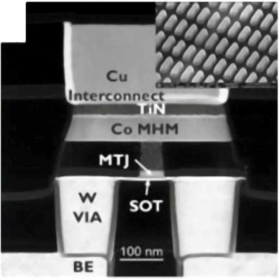
 Lateral TEM cross section view of the SOT-field-free switching-MTJ with Co magnetic hard mask (MHM).
At the 2018 Symposia on VLSI Technology and Circuits, imec demonstrated the possibility of fabricating state-of-the-art SOT-MRAM devices on 300mm wafers using CMOS-compatible processes. These SOT-MRAM devices are a class of non-volatile memories that, thanks to a high endurance and sub-ns switching speed, can potentially replace fast L1/L2 SRAM cache memories. Writing of the memory elements is performed by injecting an in-plane current in a SOT layer that is adjacent to a magnetic tunnel junction (MTJ). During write operation, a small in-plane magnetic field is required to break symmetry and ensure deterministic magnetization switching. In today’s devices, this is done by applying an external magnetic field, which is recognized as a major hurdle for the practical use of these devices.
Imec has proposed a reliable ‘field-free’ switching concept that consists of embedding a ferromagnet in the hardmask that is used to shape the SOT layer. With this ferromagnet, a small homogeneous in-plane field is induced on the free layer of the magnetic tunnel junction. “A major advantage of imec’s integrated solution compared to other proposed solutions, is the ability to separately optimize the properties of the magnetic tunnel junction and the conditions of the field-free switching”, explains Gouri Sankar Kar, program director at imec. “This ‘de-coupling’ turns our field-free switching solution into a manufacturing friendly concept, which is a major requirement for the high-volume production of SOT-MRAM devices.”
With writing speeds below 300ps and unlimited endurance (up to 1011 cycles) – measured on multiple devices across a 300mm wafer – the approach is shown to be reliable while preserving the original sub-ns writing of the SOT-MRAM devices. “This confirms the potential of the SOT-MRAM devices for replacing SRAM at low-level caches”, adds Gouri Sankar Kar. “Moreover, the new field-free switching concept can potentially be applied to other MRAM-based technologies such as spin-transfer torque MRAM (STT-MRAM) and voltage-controlled magnetic anisotropy (VCMA), and opens doors to other non-volatile logic and memory applications such as non-volatile flip-flop and non-volatile latch circuits.” Future work will focus on further reducing the energy consumption of the SOT-MRAM devices by bringing down the switching current.