Oct 13 2020
Moore’s law is essentially an empirical suggestion explaining that the number of transistors increases by two-fold every few years in integrated circuits (ICs).
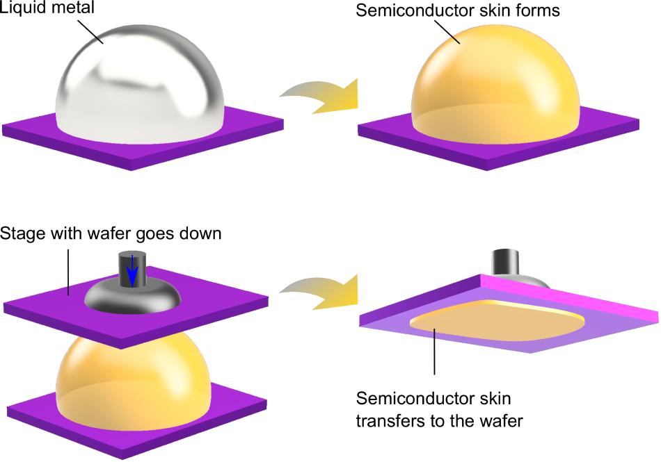
 New deposition approach: synthesizing and exfoliating (transferring onto a silicon substrate for example) 2D semiconducting MoS2. Image Credit: Arc Center of Excellence in Future Low-Energy Electronics Technologies.
But Moore’s law has begun to fail because the present generation of transistors is so compact that existing silicon-based technologies are not able to provide more prospects for shrinking.
However, Moore’s law can be resolved by resorting to two-dimensional (2D) semiconductors. Such 2D materials are so thin that they can enable the propagation of free-charge carriers, such as electrons and holes in transistors that carry the data, along an ultra-thin plane.
Through this confinement of charge carriers, the semiconductor could be easily switched off. This confinement also enables directional pathways for the charge carriers to shift without scattering, thus resulting in endlessly insignificant resistance for the transistors.
This implies that theoretically, the 2D materials can lead to the development of new transistors that do not waste energy while they are being switched on and off.
In theory, the transistors can change very quickly and can also switch off to absolute zero resistance values while they are in non-operational states.
This may sound perfect, but life is not perfect. In reality, several technological barriers still exist that must be overcome to make such ideal ultra-thin semiconductors. One of the obstacles with present-day technologies is that the deposited ultra-thin films contain so much grain boundaries that the charge carriers are bounced back from them, and as a result, the resistive loss is increased.
Molybdenum disulfide (MoS2) is one of the most interesting ultra-thin semiconductors. It has been the subject of intense research for the past 20 years for its electronic characteristics. But achieving very large-scale 2D MoS2 without any grain boundaries has been demonstrated to be a real challenge.
Utilizing any prevalent large-scale deposition technologies, grain-boundary-free MoS2, which is crucial for making ICs, is yet to be realized with tolerable maturity.
But now, scientists from the School of Chemical Engineering at the University of New South Wales (UNSW) have designed a technique to remove these grain boundaries on the basis of a novel deposition method.
This unique capability was achieved with the help of gallium metal in its liquid state. Gallium is an amazing metal with a low melting point of only 29.8 °C. It means that at a normal office temperature it is solid, while it turns into a liquid when placed at the palm of someone’s hand.
Ms Yifang Wang, Study First Author, School of Chemical Engineering, University of New South Wales
Ms. Wang continued, “It is a melted metal, so its surface is atomically smooth. It is also a conventional metal which means that its surface provides a large number of free electrons for facilitating chemical reactions.”
By bringing the sources of molybdenum and sulphur near the surface of gallium liquid metal, we were able to realize chemical reactions that form the molybdenum sulphur bonds to establish the desired MoS2.
Kourosh Kalantar-Zadeh, Study Lead Author, Arc Center of Excellence in Future Low-Energy Electronics Technologies
Kalantar-Zadeh added, “The formed two-dimensional material is templated onto an atomically smooth surface of gallium, so it is naturally nucleated and grain boundary-free. This means that by a second step annealing, we were able to obtain a very large area MoS2 with no grain boundary. This is a very important step for scaling up this fascinating ultra-smooth semiconductor.”
Currently, the UNSW team is planning to extend their techniques to produce other 2D semiconductors as well as dielectric materials to make several materials that can be utilized as different components of transistors.
The study was carried out with the help of colleagues from the University of California Los Angeles (UCLA), United States, and RMIT in Australia.
Journal Reference:
Wang, Y., et al. (2020) Self-Deposition of 2D Molybdenum Sulfides on Liquid Metals. Advanced Functional Materials. doi.org/10.1002/adfm.202005866.