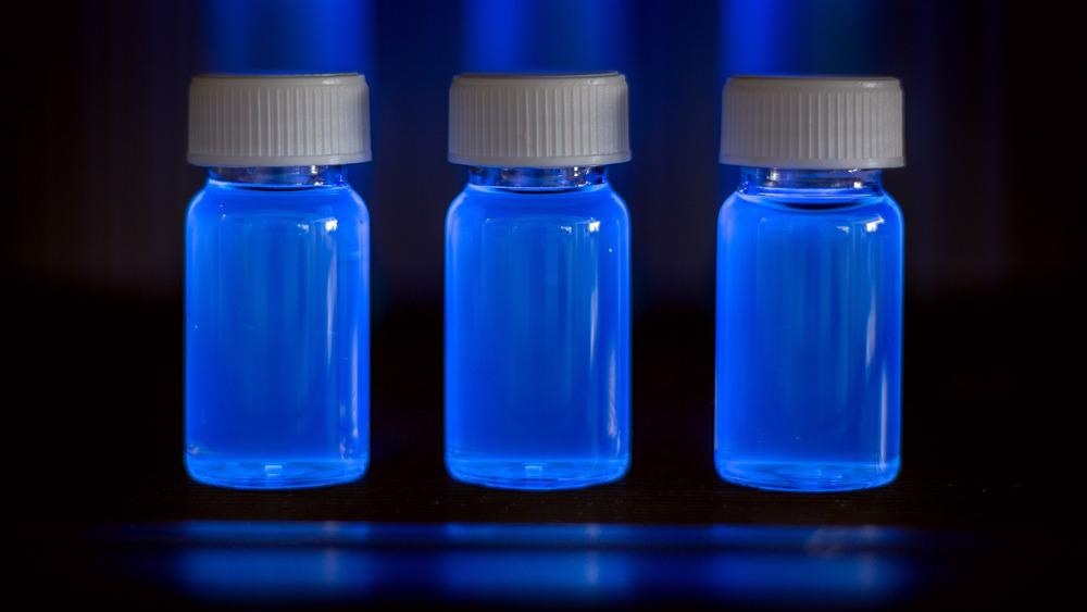
The latest research in the journal ACS Applied Nano Material focuses on the manufacturing of a drastically enhanced silicon nanowire (SiNW)-based broadband photodetector utilizing SiNW core-shell structure with hydrothermally processed nitrogen-doped graphene quantum dots (N-GQDs).

Study: Silicon Nanowire Arrays with Nitrogen-Doped Graphene Quantum Dots for Photodetectors. Image Credit: Tayfun Ruzgar/Shutterstock.com
According to the study, silicon is a naturally occurring, multipurpose, harmless semiconducting mineral with an energy bandgap that corresponds to the solar spectrum.
Material Properties
One-dimensional (1-D) SiNWs have increased study attention because of their larger surface-to-volume proportion, strong light trapping effect, quick charge transport, and high charge collecting efficiency by reducing the carrier transport path in contrast to bulk Si.
Industrial Utilization
After etching, SiNWs exhibit improved material features such as light absorption and emission, surface built-in-field amplification, electron-hole coupling, quantum confinement, and so on. As a result, photodetectors, photovoltaics high sensitivity sensors, field-effect transistors, thermoelectric devices, supercapacitors, and other devices will benefit from increased use. Reactive-ion etching can be used to create single-crystalline SiNWs.
Experimental Methods
In an airtight glass bottle, glucose and aqueous ammonia solution were mixed to create N-GQDs. The airtight glass container containing 0.325 M glucose (290 mg in 5 mL DI water) and 0.528 M ammonia (45 mg in 5 mL DI water) was then put in a cabinet. For varying reaction periods, the solution combination was placed within the container at standard temperature and ambient pressure with no light irradiation (0, 1, and 3 months). A molecular weight threshold was used to dialyze the N-GQDs generated during the 3-month reaction period.
A photodetector based on p-SiNW and nitrogen-doped graphene quantum dots (NGQDs). The MACE approach was used to produce vertically stacked SiNW arrays on a commercialized Si wafer [p-type, (100) orientated, 10-15 Ω-cm, 1 * 1 cm2 size].
N-GQDs layer was obtained on a SiNW array by spin coating 100 μL of N-GQDs on a 1 × 1 cm2 SiNW template at 3000 rpm for 30 s.
Morphological Results
The average length of the SiNW array was predicted to be 5 μm, with a diameter ranging from 20 to 200 nm. The nonuniform Au coating over the Si surface, as well as the extremely anisotropic etching during growth, account for the massive diameter dispersion.
The N-GQD XRD pattern shows a wide peak centered at 2θ = 22.5°. The corresponding particle size calculated from the Debye-Sherrer formula was ∼4.24 nm.
The high-resolution XPS N 1s spectrum was examined to further investigate the configurations of N present in the NGQDs. The N 1s peak at 398.52 eV perhaps fitted into three different peaks centered at ∼398.5, ∼ 400.2, and ∼401.5 eV, corresponding to pyridinic N (398.5 eV), pyrrolic N (400.2 eV), and graphitic N (401.5 eV), respectively.
Optical Analysis
The range of absorption spectra of N-GQDs was from 250 to 600 nm. The main distinct absorption peak at ∼277 nm arises due to the π−π* electrons transitioning. The observed broad absorption band after the 300 nm wavelength, a distinct peak at 350 nm, and a bandgap transition absorption peak at 425 nm with a long tail extending into the visible region.
Quantum Dots , what are they? How they work and what their Applications?
Video Credit: Right Vision/Youtube.com
For all four distinct templates, a wide absorption peak ranging from 250 to 500 nm is found, with an extended absorption tail into 900 nm.
Optoelectronic Results
At room temperature, all IV parameters were measured with a Keithley 4200. For light irradiation, a solar simulator with a power of 100 mW/cm2 was employed. A higher PL intensity peak value was observed. The existence of a larger degree of porosity in the SiNW array is indicated by the significantly higher PL intensity with a peak value at 655 nm.
The asymmetry of the IV curves shows the establishment of a heterojunction between the SiNWs matrix and the N-GQDs. When compared to the control SiNW device, all of the N-GQDs plated transistors show a considerable drop in photocurrent and an increase in photocurrent under visible light.
When compared to the control SiNW semiconductor, all of the N-GQDs coated gadgets show a considerable drop in dark current and an increase in photocurrent under visible light.
The creation of a band structure between N-GQDs and SiNWs might explain the huge improvement in photoresponsive properties when the reverse gate voltage is applied.
In short, Nitrogen-doped GQD (N-GQD) and p-SiNWs are synthesized using hydrothermal and MACE techniques, respectively, to create a new N-GDQ/SiNW core-shell heterostructure using a standard low-cost solution.
The optical and optoelectronic capabilities of the heterostructure were greatly enhanced by expanding the useful connection region during the KOH etching of SiNWs. In addition to photodetector applications, the heterostructure might be used in a solar cell arrangement capable of capturing the whole sunlight spectrum.
References
Mondal, H., Dey, T., & Basori, R. (2021). Silicon Nanowire Arrays with Nitrogen-Doped Graphene Quantum Dots for Photodetectors. ACS Applied Nano Materials. https://pubs.acs.org/doi/abs/10.1021/acsanm.1c0250
Disclaimer: The views expressed here are those of the author expressed in their private capacity and do not necessarily represent the views of AZoM.com Limited T/A AZoNetwork the owner and operator of this website. This disclaimer forms part of the Terms and conditions of use of this website.