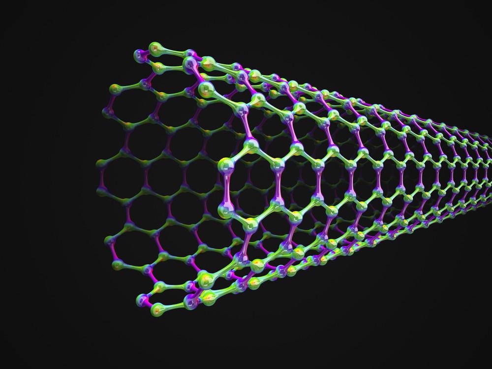
Semiconducting carbon nanotube (CNT) films represent one of the most promising channel material solutions to the fabrication of complementary metal-oxide semiconducting (CMOS) field-effect transistors (FETs). These are further explored in the journal Advanced Electronic Materials.

Study: Deep-Submicrometer Complementary Metal-Oxide-Semiconductor Transistors Based on Carbon Nanotube Films.Image Credit: Orange Deer Studio/Shutterstock.com
Semiconducting CNTs are able to provide exceptionally high mobility for both electrons and holes, while offering a stable structure and atomic layer thickness. These already impressive materials represent attractive channel material options for CMOS FETs, offering a number of advantages over traditional silicon CMOS transistors including improved performance and enhanced scaling-down limits.
CMOS technology is a core component of integrated circuits (ICs) and these typically offer excellent potential in optimizing the ICs’ performance. One of the major barriers to the development of truly symmetric CMOS FETs stems from the limited performance of short-channel n-type FETs that have been built on a foundation of solution-derived CNT films.
In order to leverage the full potential of CNT-based ICs it is necessary to develop a uniform wafer-scale semiconducting CNT film.
Over the past 5 years, solution-derived CNT randomly oriented films have been found to offer the best potential for the fabrication of both FETs and ICs due to their wafer-scale uniformity and high levels of semiconducting purity.
Unfortunately, digital CMOS ICs built on solution-derived CNT films suffer from low performance, due to the fact that n-type FETs do not perform well when operating at a sub-micrometer channel length.
New research presented in the Advanced Electronic Materials journal aims to address this issue and overcome this barrier.
More on Nanotubes: Flexible Batteries Employing Carbon Nanotubes
Two approaches are typically employed in order to develop n-type FETs based on CNT films, both of which aim to optimize the Schottky barrier—a potential energy barrier for electrons that is formed at the junction of metal and semiconductor. Ideally, the Schottky barrier should be low in order to allow electrons to pass through this easily.
Doping-free technology is a widely recognized approach that uses a low work function metal as the source and drain in order to form a low Schottky barrier for electrons and a high barrier for holes. The other approach involves doping the CNT film channel with chemical dopants or covering this with a dielectric dipole layer.
Applied in isolation, these methods have proven to be insufficient for the production of n-type FETs because they result in a high Schottky barrier.
The researchers, therefore, explored the possibility of combining these two methods to achieve a notable FET performance improvement, using these to fabricate solution-derived CNT films and develop symmetric CMOS FETs at sub-micrometer lengths.
The researchers opted to use scandium (Sc) metal as a contact due to its potential to realize a low Schottky barrier for electrons. They also employed a specific yttrium-doping method on the CNT channel in order to further reduce the Schottky barrier at the contact points.
It was important to carefully manage the thickness of the yttrium film deposited on the CNT channels. A balance had to be struck between ensuring a suitable doping effect and ensuring that there was no degradation of the n-type FETs; for example, a reduction of the on/off ratio.
How Carbon Nanotubes Will Change the World
Video Credit: Real Engineering/Youtube.com
This novel fabrication approach allowed the construction of 150 nm gate length CMOS FETs that offered both high and symmetric performance.
For example, the study found that this approach could offer on-state current density Ion up to ≈270 µA µm-1. Not only that, but the method delivered a peak transconductance gm above 100 μS µm-1 for both n- and p-FETs.
These findings were confirmed and evaluated for their potential use in practical applications via a range of circuit- and system-level benchmarking approaches. These approaches were based on the use of the experimental CMOS transistors.
Perhaps most notably, these deep-sub-micrometer CMOS FETs also demonstrated excellent results in terms of energy efficiency, with tests highlighting an almost 4x performance improvement while using the same amount of power as the latest reported CNT CMOS FETs with a 2 GHz working frequency.
The researchers also highlighted the potential to improve the FETs’ performance even further by eliminating polymer residues to ensure a completely clean interface between CNTs and metal, identifying this as a potential pathway for future study.
The study’s results represented the best performing CNT CMOS FETs produced thus far and offer excellent potential for the further optimization and application of these already highly beneficial components, particularly in the construction of high-performance integrated circuits.
Disclaimer: The views expressed here are those of the author expressed in their private capacity and do not necessarily represent the views of AZoM.com Limited T/A AZoNetwork the owner and operator of this website. This disclaimer forms part of the Terms and conditions of use of this website.
Source:
Shi, H., Ding, L., Zhong, D., Peng, L.-M., Zhang, Z., Deep-Submicrometer Complementary Metal-Oxide-Semiconductor Transistors Based on Carbon Nanotube Films. Adv. Electron. Mater. 2021, 2100751. https://onlinelibrary.wiley.com/doi/10.1002/aelm.202100751