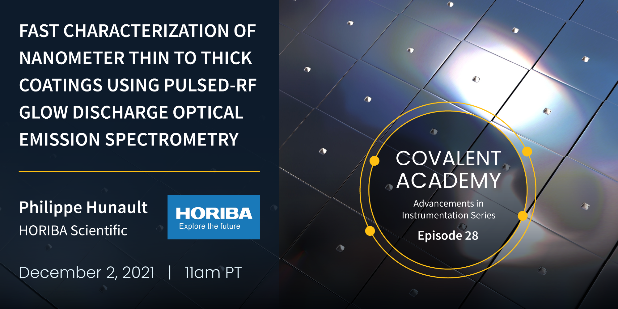
HORIBA Scientific, a global leader in the production of high-performance spectroscopy systems and solutions, is proud to be hosting a joint webinar with Covalent Metrology on Thursday, December 2nd at 2PM EDT.

Image Credit: Horiba Scientific
The presentation, entitled, “Fast Characterization of nm Thin to Thick Coatings using Pulsed-RF Glow Discharge Optical Emission Spectrometry,” will show this technique’s ability to characterize both conductive and non-conductive layers and coatings from nm to 100+ microns thickness.
After reviewing the theory and the instrument configuration, this presentation will be focused on a large variety of applications, including Li Ion Batteries, Energy Storage, Photovoltaics, PVD, CVD and Organic Coatings, Platings, Thin and Thick Oxides, Failure Analysis and more.
To register, to go: https://covalentmetrology.com/covalent_event/fast-characterization-of-nanometer-thin-to-thick-coatings-using-pulsed-rf-glow-discharge-optical-emission-spectrometry/
HORIBA Scientific has partnered with Covalent Metrology, a leading North American provider of analytical services, to expand engineering and scientific access to world-class expertise and chemical analysis instruments. In addition to co-hosting this webinar, Covalent and HORIBA have opened the HORIBA Scientific North American Demonstration Lab at Covalent’s Silicon Valley headquarters. This showroom is HORIBA’s first demonstration lab with a partner in North America and adds to our application / demo labs in our corporate offices. The lab will showcase top-of-line spectroscopy solutions, and bolster the companies’ mutual efforts to develop methods for new chemical analysis applications. With access to new, cutting-edge instruments from HORIBA, Covalent’s team of experts will be better able to support clients with more accurate and powerful chemical analysis capabilities.