Mitsui Mining and Smelting Co., Ltd (President and Representative Director: Takeshi Nou; hereinafter “Mitsui Kinzoku”) and GEOMATEC Co., Ltd (CEO: Kentaro Matsuzaki; hereinafter “GEOMATEC”) have been working together to establish a mass production system for the commercialization of HRDP®,1 a specialty carrier for next-generation semiconductor packaging. Mitsui Kinzoku is pleased to announce that we have decided to invest in a second production line in GEOMATEC’s Ako plant to increase production capacity and expand the DOE facility.
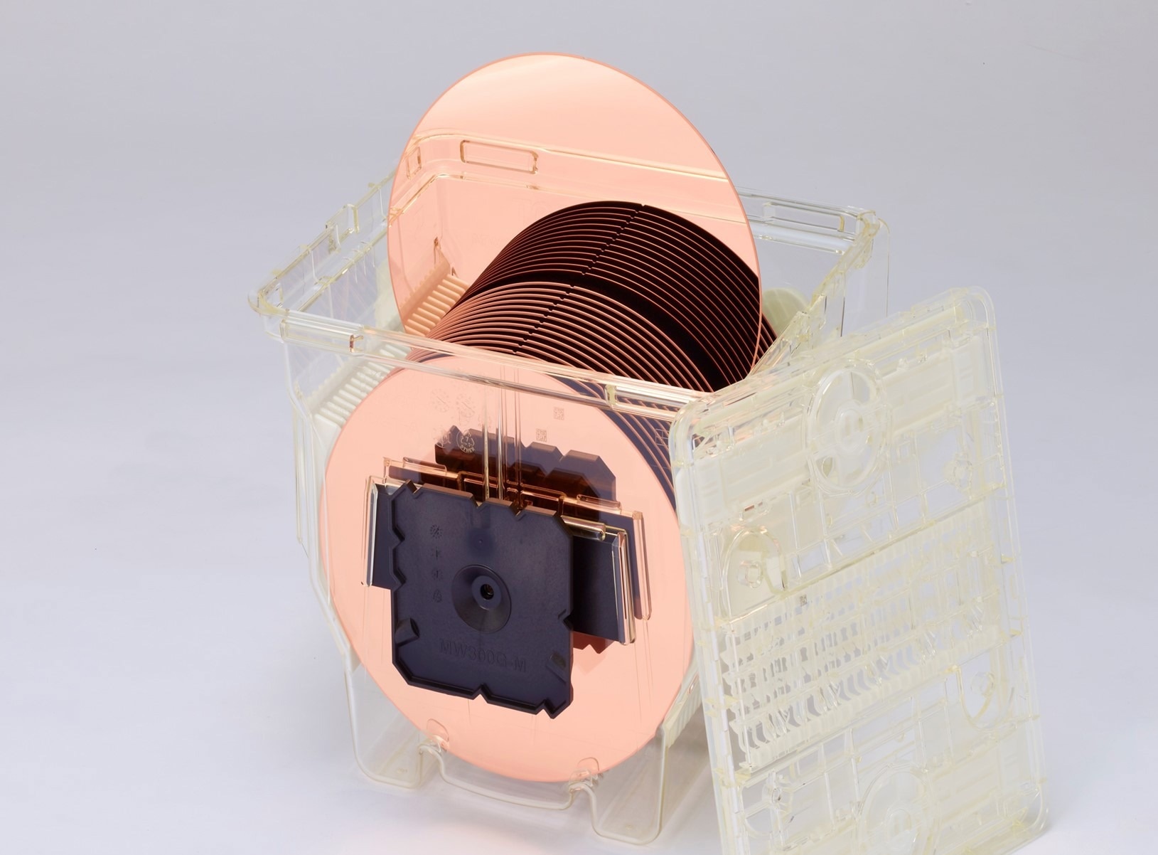
 300mm wafer type HRDP® products (In a special case for shipping products) Image Credit: Business Wire
Developed by Mitsui Kinzoku, HRDP® is a specialty carrier that achieves an ultra-high-density design with an L/S of 2/2 μm or less which is necessary for next-generation semiconductor packaging.
Currently, several major semiconductor companies have begun the full-scale development of their next-generation semiconductor packages using HRDP®. In response to this, Mitsui Kinzoku has decided to further improve quality and increase production capacity by introducing a second HRDP® line at GEOMATEC’s Ako plant, scheduled to start operation in 2025. At the same time, GEOMATEC will invest in the thin-film process used on this second line.
In addition, by expanding the DOE facility2 already in operation, we will accelerate joint development with major semiconductor companies using HRDP®. This will enable customers to shorten cycle times.3
With the installation of the second line and the expansion of the DOE facility, we will be able to respond quickly to the increasing demand for development and move toward the adoption of HRDP® and the expansion of its use in mass production in the next-generation semiconductor market in the future. This capital investment will be made in steps from 2023 to 2025.
Based on our purpose, “We promote the well-being of the world through a spirit of exploration and diverse technologies.” We will contribute to the semiconductor packaging market by expanding our HRDP® business and contribute to the creation of a sustainable society through our business activities.
Explanation of Terms
- High Resolution Debondable Panel.
- DOE: Design of Experiments. A development facility for identifying and resolving issues in advance by verifying customer designs.
- The number of processes and the time required to manufacture a semiconductor package. If these can be reduced, optimal semiconductor device manufacturing efficiency can be achieved.
- Re-Distribution Layer
References
Development of HRDPTM Material for Formation of Ultra-Fine Circuits with Glass Carrier for Fan Out Panel Level Package (release dated January 25, 2018) https://www.mitsui-kinzoku.com/Portals/0/resource/uploads/topics_180125e.pdf?TabModule1277=1
Initiation of the Mass Production of HRDP®, a Special Glass Carrier for Next-Generation Semiconductor Packaging Devices (release dated January 25, 2021) https://www.mitsui-kinzoku.com/LinkClick.aspx?fileticket=rh%2bDH1M4W%2bs%3d&tabid=278&mid=824&TabModule1277=1
Mass Production of the HRDP® Special Carrier for Next-generation Semiconductor Packaging Device begins for the Overseas market (release dated December 14, 2021) https://www.mitsui-kinzoku.com/LinkClick.aspx?fileticket=rf%2bLsUEKH8g%3d&tabid=278&mid=824&TabModule1277=1
Video illustrating the chip last process using HRDP® https://www.youtube.com/watch?v=vHhng-NV9QA