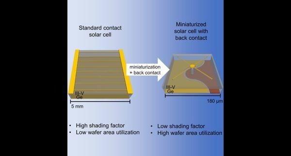
Photo showing the difference between a standard solar cell and a miniaturized solar cell. Image Credit: University of Ottawa
The cells, which are twice as thick as a hair strand, provide substantial benefits over traditional solar technologies, including a 95% reduction in electrode-induced shadowing and a threefold potential reduction in energy production costs.
The scientific discovery, spearheaded by Mathieu de Lafontaine, a part-time physics professor and postdoctoral researcher at the University of Ottawa, and Karin Hinzer, vice-dean of research and holder of the University Research Chair in Photonic Devices for Energy at the Faculty of Engineering, opens the door to a new phase of electronic device miniaturization.
The University of Ottawa, the Université de Sherbrooke in Quebec, and the Laboratoire des Technologies de la Microélectronique in Grenoble, France, collaborated on the production of micrometric photovoltaic cells.
These micrometric photovoltaic cells have remarkable characteristics, including an extremely small size and significantly reduced shadowing. Those properties lend themselves to various applications, from densification of electronic devices to areas such as solar cells, lightweight nuclear batteries for space exploration and miniaturization of devices for telecommunications and the internet of things.
Karin Hinzer, University Research Chair, Photonic Devices for Energy, University of Ottawa
A Breakthrough with Huge Potential
This technological breakthrough promises significant benefits for society. Less expensive, more powerful solar cells will help accelerate the energy shift. Lightweight nuclear batteries will facilitate space exploration, and miniaturization of devices will contribute to the growth of the internet of things and lead to more powerful computers and smartphones.
Mathieu de Lafontaine, Postdoctoral Researcher, University of Ottawa
He added, “The development of these first back-contact micrometric photovoltaic cells is a crucial step in the miniaturization of electronic devices.”
Hinzer added, “Semiconductors are vital in the shift to a carbon-neutral economy. This project is one of many research initiatives that we are undertaking at the Faculty of Engineering to achieve our societal goals.”
Semiconductors are part of two of the four strategic research areas at the University of Ottawa, which are forming a sustainable environment and the digital world, and three of the five research areas at the Faculty of Engineering, which are information technologies, photonics, and emerging materials.
This multinational collaboration between France and Canada paves the path for a future in which technology will advance to unprecedented levels of power and accessibility while demonstrating the significance of innovation and research in micromanufacturing. It also represents a significant turning point in the history of science and technology worldwide.
The Natural Sciences and Engineering Research Council of Canada, the Fonds de recherche du Québec Nature et technologies, Prompt Québec, the Horizon Europe Framework program, and STACE Inc. provided funding for this project.
Journal Reference
de Lafontaine, M., et al. (2023) 3D interconnects for III-V semiconductor heterostructures for miniaturized power devices. Cell Reports Physical Science. doi:10.1016/j.xcrp.2023.101701.