One of the main challenges in developing semiconductor chip technology is making electronic components smaller and more effective. This difficulty is most noticeable in lithography, which is the process of forming complex patterns on semiconductor materials, or wafers, to produce chips.
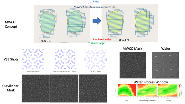
 Concept of mask/wafer co-optimization by moving the shot with mask and wafer double simulation to minimize wafer error. VSB shot configurations and its corresponding pattens on mask. MWCO mask and its wafer print. Wafer Process Windows shows MWCO improved process window by 2×. Process window is a key measurement of wafer print quality. Image Credit: The Authors doi 10.1117/1.JMM.23.1.011207
In lithography, patterns are made on semiconductor wafers using a type of template known as a photomask, or just mask. The industry is always searching for ways to increase wafer and mask manufacturability and resolution since they will lead to quicker chips with a greater yield of chips that work properly.
By altering each mask design, computational lithography techniques like optical proximity correction (OPC) have made significant strides in resolving these issues and enhancing mask and wafer printing.
Many lithography-related problems associated with advanced chips have been identified to have a possible answer in inverse lithography technology (ILT), a mathematically rigorous inverse technique that predicts the mask shapes that would yield the appropriate on-wafer outputs.
Numerous studies have shown that curvilinear ILT mask designs, in particular, yield the greatest wafer performance since its inception more than ten years ago.
Nevertheless, until recently, this computational technique’s real applicability was restricted to crucial “hotspots” on chips due to its related runtimes. An entirely novel, specially designed system was shown in 2019; it included a novel GPU-accelerated method that simulates a single, enormous GPU/CPU pair capable of simultaneously computing a whole full-chip ILT solution.
With this innovative method, which was methodically created for GPU acceleration and ILT, full-chip ILT became a feasible outcome in manufacturing.
This method, however, was dependent on multi-beam mask writing, a significant advancement in mask writing that is pixel-based and, hence, write-time independent of form. The last challenge was whether the advantages of full-chip, curvilinear ILT could be extended to variable-shaped beam (VSB) mask writers, which comprise the bulk of mask writers in use today and write rectilinear (and occasionally triangular) forms instead of pixels.
Complex mask patterns can be problematic because writing the enormous number of little rectangles required to generate them would take too long, even if VSB writers can quickly build bigger rectangular forms by writing one rectangular shot at a time.
The team at D2S, Inc. developed a technique known as mask wafer co-optimization (MWCO), which they reported in the Journal of Micro/Nanopatterning, Materials, and Metrology.
Three key findings emerged from their work: (1) both the mask writer and the wafer scanner are low-pass filters; (2) overlapping shots influenced by mask/wafer simulation can create curvilinear shapes with fewer shots; and (3) by targeting the wafer pattern rather than the mask pattern, one can establish much simpler shots to print the correct wafer pattern.
This double simulation is used to repeatedly enhance wafer print quality while adjusting VSB shot edges to create rectilinear target mask shapes with a known and acceptable shot count that can be written on a VSB writer.
Compared to Micron OPC, D2S and Micron Technology have shown that MWCO can enhance the wafer process window by two times and minimize wafer variation by three times, showing a significant improvement in the accuracy and dependability of the lithography process. A complete curvilinear ILT mask can be written in less than 12 hours, meeting the demands of high-volume manufacturing.
This implies that, even in the absence of a multi-beam mask writer, semiconductor manufacturers can now develop chips that are not only smaller but also more powerful and consume less power.
Journal Reference:
Peng, L., et. al. (2024) Make the impossible possible: use variable-shaped beam mask writers and curvilinear full-chip inverse lithography technology for 193i contacts/vias with mask-wafer co-optimization. Journal of Micro/Nanopatterning, Materials, and Metrology. doi:10.1117/1.JMM.23.1.011207.