Sponsored by HORIBAOct 24 2013
Graphene is a unique material that contains single molecular layers of highly crystalline graphite. This material was first reported in 2004 and represents the basic structural element of carbon allotropes including carbon nanotubes, graphite and fullerenes.
Graphene has superior electron transport properties, making it promising material for future nanoelectronic devices. The material also exhibits high thermal conductance and high mechanical strength, which is roughly 200 times greater than steel. It is also used in the development of ultra-fast nanoscale transistors that operate in the THz region. Owing to its size and optical properties, graphene is not visible on majority of substrates.
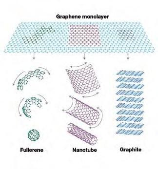
Figure 1. Graphene is the basic structural element of carbon allotropes such as fullerenes, nanotubes or graphite.
Raman Spectroscopy
However, in order to study graphene-based devices, it is important to distinguish the number of graphene layers and quantify the effect of disorder on its properties. Raman micro spectroscopy provides a suitable and reliable technique to determine both these properties. The high spectral and spatial resolution of Raman spectroscopy, combined with high structural selectivity and non-destructive nature of this technique make it a standard characterization tool in the rapidly growing field of graphene.
The Raman spectrum of graphene, as shown in figure 2, includes several peaks which are well distinguished and understood. This article describes each peak in detail.
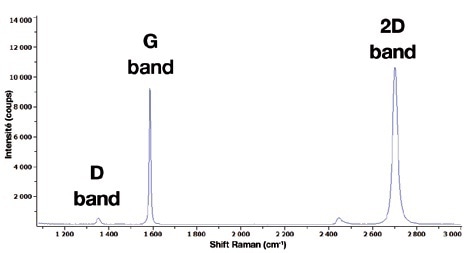
Figure 2. Raman spectrum of graphene
The G and D Bands
G band is the main spectral feature of graphene and appears close to 1580cm-1. It is very sensitive to strain effects and indicates the number of graphene layers. The G band position moves to lower frequencies, as the number of layers increases, as shown in figure 3. However, no major change is observed in spectral shape. In addition, the G band is sensitive to doping and both the line width and frequency of this peak can be employed to check the doping level.
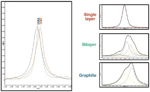
Figure 3. G band and 2D band are commonly used to determine the number of graphene layers
The D band, also known as the disorder band, occurs due to lattice motion away from the middle of the Brillouin zone and its presence between 1270 and 1450cm-1.
The 2D Band
Also dubbed as G, the 2D band is a second order two phonon process and has a strong frequency dependence on the excitation laser because of a double resonance process which joins the phonon wave vector to the electronic band structure. This peak occurs at about 2700cm-1 for a 514nm laser excitation, as shown in figure 2. However, its behaviour is more intricate in comparison to the frequency shift seen for the G band.
Raman Imaging of Graphene Layers
It is often difficult to localise graphene optically and an optical microscope proves ineffective to determine the number of graphene layers or defects. With a high spatial resolution, Raman imaging offers a quick and reliable technique to collect such information.
Using the XploRA Raman spectrometer with a 532nm laser excitation, a Raman map of a graphene sample on a SiO2/Si substrate has been carried out. Two different ways for processing the information, such as peak-fitting treatments and multivariate modelling are described below.
Multivariate Modelling
Using the modelling function of Labspec 5, the distribution of a multilayer (in red) and the bilayer (in green) are easily collected. Since the D band was also identified at some edges, a third spectrum denotes that species was also utilized to fit the map (in pink).
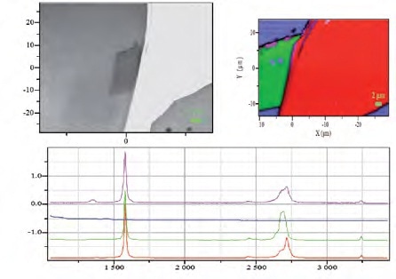
Figure 4. Optical micrograph (top left), Raman image of graphene bilayer (in green), multilayer graphene (in red), edges (in pink) and SiO/Si substrate (in blue) (top right) based on the modelling algorithm using "pure" spectra of the different regions (bottom).
Maps based on band fitted parameters, such as area, amplitude, peak position, and/or band width, can also be constructed. In figure 5, the images on the right side of the figure were made by using the combined intensity of each of the lines in the spectra. This example shows the usefulness of Raman imaging for validating the homogeneity of graphene layers.
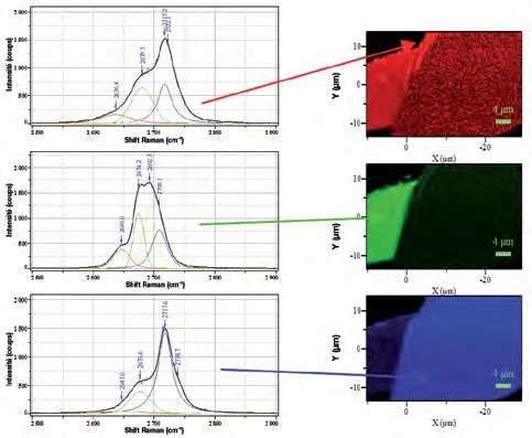
Figure 5. Raman image (right) are based on band-fitted parameters: the intensity of the color in each image is based on the integrated intensity of the spectrum at each point.
Graphene: A Suitable Raman Substrate
Recent studies have shown that graphene could serve as a suitable Raman substrate for studying complex samples. The material can help suppress strong intrinsic fluorescence. Moreover, when depositing a sample onto a graphene layer, a Raman enhancement effect can be observed.
Surface Enhanced Raman Scattering
Enhancement techniques are mainly based on resonant surface enhanced Raman scattering (SERS) and Raman scattering (RRS). The requirement for a substrate that is biocompatible, chemically inert, and capable of Raman enhancement is a major technological objective and graphene serves as a suitable material.
Conclusion
Raman spectroscopy has proven to be an effective technique for analyzing the innovative nanomaterial, graphene. This technique has also helped in identifying some unique properties of graphene as a Raman substrate for the suppression of fluorescence. In future, graphene may partially substitute silicon in computer chips and microcircuits. However, in order to gain a better insight into the material’s quality characteristics, rapid and reliable techniques that provide the right property measures are required.

This information has been sourced, reviewed and adapted from materials provided by HORIBA.
For more information on this source, please visit HORIBA.