Researchers and industries have been using transmission electron microscopy (TEM) to study semiconductors' stacking and dislocation faults. This article considers the analysis of crystal structures.
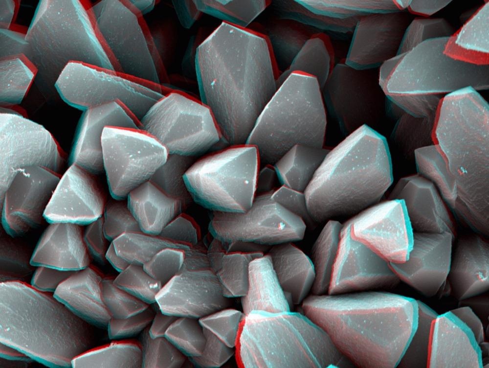
Image Credit: Image Source Trading Ltd/Shutterstock.com
Crystal defects such as stacking faults and dislocations determine the mechanical properties of materials. They may also significantly impact semiconductor electronic properties because they act as charge carrier scattering centers in light-emitting devices and solar cells. The characterization of dislocations in terms of density, dislocation type, and distribution is essential to understanding the mechanical properties.
Electron Microscopy and Crystal Structure
EM is widely used to analyze the crystal size and morphology among all other structural features of crystals. TEM and scanning EM (SEM) images can directly observe the particle sizes in the crystal. However, EM's inherent disadvantage is that the number of particles that can be examined is always limited. The other limitation is that it does not provide an accurate estimate of the crystallite size and any indication of the length of the crystals.
Many crystals have well-defined facets and appear as polyhedra. SEM images, which provide a 3D impression with image contrasts from different facets, can help study these polyhedra. However, unless electron backscatter diffraction (EBSD) is used, determining the crystal orientations of the facets from SEM images is not possible.
However, it is difficult to see the particle morphology in SEM images due to a resolution limit if the particle size is very small. Instead, TEM images are frequently used, but their application makes it difficult to recognize polyhedra. Software analysis can also be used to study the polyhedra in the crystals.
EM can help analyze the chemical composition of crystal particles, and it can also be used to study crystal areas. Electron energy loss spectroscopy, elemental mapping, and elemental distribution in a particle can also be equipped with EM to get detailed results on variation in the composition of samples.
Even though the reciprocity theorem suggests that scanning transmission EM (STEM) and TEM imaging have the same diffraction contrast, STEM is not widely used for defect characterization. As compared to other methods of crystal elemental analysis, STEM-based fundamental analysis has a significant advantage. This is because STEM reduces the interconnection between the electron beam and the sample, resulting in significantly less sample damage.
Defect Study
The use of EM to investigate defects in solids is a common and important research field. Point defects, layered defects, anti-phase defects, twin defects, stacking faults, domain structures, and dislocations are among the common defects that researchers and industry study.
During anti-phase and twin defects analysis, it is observed that both of them have identical planer boundaries. Their presence is confirmed in crystals by displaying the dark contract line on the boundary when the specimens are viewed parallel during TEM and SEM. It must also be noted that the lattice patterns shift by half of a unit cell on both sides of the boundary when these defects are present in the crystals. With regard to the TEM analysis of the defects, no lattice fringes are visible, but the change in image contrast validates the presence of the defect.
EM also helps in the study of point defects in the crystals. Notably, different arrangements are required to study the different types of point defects in the crystals with EM. The images of the point defect can also be used to understand other important parameters in crystals.
The study of the point defects is also significant to understanding crystal growth, and its TEM imaging is often difficult to quantitatively measure point defect concentration and structure. The TEM relies on the diffraction and interference effects, and it is not very sensitive to randomly distributed point defects. Additionally, the TEM samples have a thickness equivalent to a unit cell, so studying a point defect is difficult. However, using SEM and high-resolution TEM points, defects in crystals are studied effectively.
Recent Studies
In a recent study published in the journal Critical Reviews in Solid State and Material Science, researchers explored three crystallographic analyses in SEM: electron backscatter diffraction, electron channeling contrast imaging, and transmission Kikuchi diffraction. According to researchers, three methods and different analysis techniques must be used for accurate crystal study by electron microscopy.
In another study published in the journal Advanced, Structural and Chemical Imagining, researchers systematically analyzed dislocation Burger vectors and displacement vectors of crystals using an SEM and low kilo-electron volts (KeV) STEM. The experiments were conducted in a specially configured instrument that allowed the researchers to control the specimen orientation and set up two-beam conditions.
More from AZoM: Microchannel Plate Detectors in Electron Spectrometers
References and Further Reading
Rafael Borrajo-Pelaez & Peter Hedström (2018) Recent Developments of Crystallographic Analysis Methods in the Scanning Electron Microscope for Applications in Metallurgy, Critical Reviews in Solid State and Materials Sciences, 43:6, 455-474, https://www.tandfonline.com/doi/full/10.1080/10408436.2017.1370576
Sun, C., Müller, E., Meffert, M. et al. Analysis of crystal defects by scanning transmission electron microscopy (STEM) in a modern scanning electron microscope. Adv Struct Chem Imag 5, 1 (2019). https://link.springer.com/article/10.1186/s40679-019-0065-1
Zhou, W. and Greer, H.F. (2016), What Can Electron Microscopy Tell Us Beyond Crystal Structures?. Eur. J. Inorg. Chem., 2016: 941-950. https://chemistry-europe.onlinelibrary.wiley.com/doi/10.1002/ejic.201501342
Disclaimer: The views expressed here are those of the author expressed in their private capacity and do not necessarily represent the views of AZoM.com Limited T/A AZoNetwork the owner and operator of this website. This disclaimer forms part of the Terms and conditions of use of this website.