Scientists need access to reliable, accurate equipment that can resolve space, time, and frequency as well as correlate form and function to progress their understanding of complicated samples and create novel materials.
The Thermo Scientific Spectra 300 (S)TEM, the highest resolution, aberration-corrected scanning transmission electron microscope, is now available for all materials science applications.
Spectra 300 Transmission Electron Microscope Advantages
Every Spectra 300 (S)TEM is supplied with new platforms that provide the best imaging quality and an unparalleled degree of mechanical stability through passive and (optional) active vibration isolation.
The device sits in a redesigned enclosure with a built-in screen display for easy loading and removal of specimens. Maximum flexibility for various room configurations is possible with full modularity and upgradeability between uncorrected and single-corrected setups with variable heights.
Spectra 300 Transmission Electron Microscope Features
High Energy Resolution Sources Available on the Spectra 300 (S)TEM
An ultra-high-energy resolution X-FEG/UltiMono or high-energy resolution X-FEG/Mono can be added to the Spectra 300 (S)TEM as an optional accessory. The monochromators of both sources are automatically excited and tuned to attain the greatest energy resolution on each configuration utilizing the OptiMono or OptiMono+, respectively.
It is possible to automatically tune the X-FEG/Mono from 1 eV down to 0.2 eV and the X-FEG/UltiMono from 1 eV down to <30 meV. To accommodate a maximum range of samples, both sources can be operated from 30 and 300 kV.
Both can also be operated in standard mode, with the monochromators turned off, to support studies that demand high brightness (such as STEM EDS mapping, ultra-high-resolution STEM, or high total current investigations like TEM imaging) without compromising the system's other specifications.
Thanks to its flexibility, the Spectra 300 (S)TEM may operate in environments where a wide variety of experiments are anticipated to be conducted on a single system.
Also Configurable With the Ultra-High Brightness X-CFEG Source
There is an option to power the Spectra 300 (S)TEM with a new cold field emission gun (X-CFEG). The X-CFEG can operate between 30 and 300 kV and has very high brightness (>>1.0 x 10⁸ A/m2/Sr/V*) and minimal energy spread (<0.4 eV).
This delivers concurrently high-resolution STEM imaging with high probe currents for rapid acquisition, high throughput STEM analytics in tandem with high-resolution STEM imaging at high probe currents.
X-CFEG and the S-CORR probe aberration corrector work together to routinely provide sub-Angstrom (<0.8 Å) STEM-imaging resolution with probe currents exceeding 1000 pA.
![Si[110] HAADF images taken with the X-CFEG/S-CORR combination; probe currents range from 0.016 nA (left) up to 1 nA (right) while maintaining <76 pm STEM resolution.](https://www.azom.com/images/equipments/EquipmentImage_8829_17059084472814124.jpg)
Si[110] HAADF images taken with the X-CFEG/S-CORR combination; probe currents range from 0.016 nA (left) up to 1 nA (right) while maintaining <76 pm STEM resolution. Image Credit: Thermo Fisher Scientific – Electron Microscopy Solutions
To accommodate the largest range of specimens and studies, probe currents can also be flexibly tuned from <1 pA up to the nA range with fine control of the gun and condenser optics, all with minimal impact on the probe aberrations.
To preserve the probe current, the sharp tip must regenerate periodically, or "flash," just like any other cold field emission source. The X-CFEG tip only needs to flash once a working day, which saves the tip time of less than a minute. Even in the highest imaging conditions, there is no discernible effect on the probe aberrations, and the daily tip flashing procedure does not affect the tip lifetime.
This new generation X-CFEG is a distinctively all-purpose, yet high-performance, C-FEG. It generates enough total beam current (>14 nA) to handle traditional TEM imaging investigations (for example, in situ) with large parallel probes.
The X-CFEG's adaptability is enhanced by its capacity to modify the energy resolution by adjusting the extraction voltage.
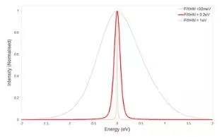
In the below example, the energy resolution was set to 0.39 eV, with <500 pA of probe current, and 0.31 eV, with >300 pA of probe current.
Without the need for a monochromator on core loss edges, extensive analysis of the Energy Loss Near Edge Structure (ELNES) study is possible as high probe currents are maintained with high energy resolution. The HAADF image of DyScO3 shows that the spatial resolution is not compromised (in this example, <63 pA).
This implies that STEM EELS studies with high spatial resolution, energy resolution, and signal-to-noise ratio can now be conducted.
The extraction voltage used in the experiment has no impact on the tip's lifetime.
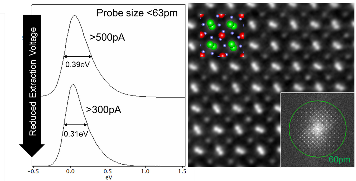
The energy resolution of the ultra-high brightness X-CFEG can be adjusted using the extraction voltage. In the case above, it varied between 0.39eV (with <500pA of probe current) and 0.31eV (with >300pA of probe current). The spatial resolution, as demonstrated in the HAADF image of DyScO3, remains unaffected (in this case <63pA). Sample courtesy Professor L.F. Kourkoutis, Cornell University. Image Credit: Thermo Fisher Scientific – Electron Microscopy Solutions
Providing the Highest Resolution STEM Imaging Performance
With the latest 5th-order probe aberration correction, improved mechanical stability, and high-resolution (S-TWIN) wide-gap pole piece, this instrument achieves the best STEM resolution requirements available in the market.
The Spectra 300 (S)TEM, with X-FEG/Mono or X-FEG/UltiMono, provides resolution specifications of 50 pm at 300 kV, 96 pm at 60 kV, and 125 pm at 30 kV with 30 pA of probe current or 100 pA with the X-CFEG.
![Ultra-high resolution HAADF STEM imaging on a Spectra 300 (S)TEM. GaN[212] imaged at 300 kV with 40.5 pm Ga-Ga dumbells resolved as well as 39 pm resolution in the FFT. The image was collected on a wide gap S-TWIN pole piece with 30 pA of probe current.](https://www.azom.com/images/equipments/EquipmentImage_8829_17059084642419453.jpg)
Ultra-high resolution HAADF STEM imaging on a Spectra 300 (S)TEM. GaN[212] imaged at 300 kV with 40.5 pm Ga-Ga dumbells resolved as well as 39 pm resolution in the FFT. The image was collected on a wide gap S-TWIN pole piece with 30 pA of probe current. Image Credit: Thermo Fisher Scientific – Electron Microscopy Solutions
Unprecedented Sensitivity With the Panther STEM Detection System
The Panther STEM detection system, which consists of new data acquisition architecture and two new solid-state, eight-segment ring and disk STEM detectors (with a total of 16 segments), has completely redesigned STEM imaging on the Spectra (S)TEM. Access to advanced STEM imaging capabilities with the sensitivity to quantify single electrons is provided with new detector geometry.
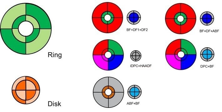
The 16 segmented ring and disk detectors of the Panther STEM detection system allow for a range of STEM signals without the need for multiple detectors. Image Credit: Thermo Fisher Scientific – Electron Microscopy Solutions
To enable imaging of materials sensitive to beams, the entire signal chain has been fine-tuned and optimized to deliver extraordinary signal-to-noise imaging capabilities with incredibly low doses.
The entirely redesigned data acquisition infrastructure can combine various detector segments and could allow for the arbitrary combination of detector segments in the future, yielding new STEM imaging techniques and uncovering data that is unavailable with traditional STEM methods. The architecture is scalable and offers an interface for synchronizing several spectroscopic and STEM signals.
![Comparison SrTiO₃ [001] HAADF images taken with the Panther STEM detection system with 3 pA, 1.3 pA and <1 pA of probe current. Even with probe currents <1 pA, the signal-to-noise ratio in the image allows automation routines like OptiSTEM+ to correct 1st and 2nd order aberrations in the probe forming optics, delivering sharp images.](https://www.azom.com/images/equipments/EquipmentImage_8829_17059084782797223.jpg)
Comparison SrTiO₃ [001] HAADF images taken with the Panther STEM detection system with 3 pA, 1.3 pA, and <1 pA of probe current. Even with probe currents <1 pA, the signal-to-noise ratio in the image allows automation routines like OptiSTEM+ to correct 1st and 2nd order aberrations in the probe-forming optics, delivering sharp images. Image Credit: Thermo Fisher Scientific – Electron Microscopy Solutions
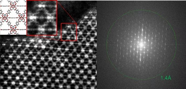
Extreme low-dose imaging of the metal organic framework (MOF) UiO 66 on the Spectra 300 (S)TEM. A probe current of <0.5 pA was used in combination with iDPC and the Panther STEM detection system to image atomic level details in this highly dose-sensitive material with a spatial resolution of 1.4 Å. The image is a single shot with a frame time of 23.5 seconds (Specimen courtesy of Professor Y. Han, King Abdullah University of Science and Technology). Image Credit: Thermo Fisher Scientific – Electron Microscopy Solutions
Advanced STEM Imaging Capabilities
To gather 4D STEM data sets, the Spectra 300 (S)TEM can be coupled up with a Thermo Scientific Ceta Camera with speed enhancement or an electron microscope pixel array detector (EMPAD).
The EMPAD is the best detector for 4D STEM applications because of its 30–300 kV capability, great dynamic range (1:1,000,000 e- between pixels), high signal-to-noise ratio (1/140 e-), and fast speed (1100 frames per second) on a 128 × 128-pixel array.
For 4D STEM applications requiring more pixels and the combination of EDS analysis with each point in the STEM scan, the Ceta Camera with speed enhancement provides an alternative. For applications like strain monitoring, this system offers diffraction patterns with a greater resolution (up to 512 × 512 pixels).
The EMPAD detector can be used for a wide variety of applications. On the left, it is used to extend spatial resolution (0.39 Å) beyond the aperture-limited resolution at low accelerating voltages (80 kV) in a bi-layer of the 2D material MoS₂ (Jiang, Y. et al. Nature 559, 343–349, 2018). On the right, it is used to independently image dark field reflections, revealing the complex microstructure of the precipitates in a superalloy (Sample courtesy Professor G. Burke, University of Manchester). Image Credit: Thermo Fisher Scientific – Electron Microscopy Solutions
Spectroscopic Flexibility With the Spectra 300 (S)TEM
The Spectra 300 (S)TEM provides the spectroscopic versatility to meet the broadest range of analytical needs, from high-throughput, high signal-to-noise ratio elemental mapping in EDS and EELS to oxidation state and surface phonon probing with ultra-high-resolution EELS.
The user has the freedom to configure the Spectra 300 (S)TEM to meet their research needs by selecting from three different sources with differing energy resolution (X-FEG Mono, X-FEG UltiMono, and X-CFEG), two different EDS detector geometries (Super-X and Dual-X), and a variety of Gatan Continuum spectrometers and energy filters.
Various detector geometries are available in the Thermo Scientific EDS detector range to meet users' experimental needs and enhance EDS results. Quantifiable data is produced by the symmetric design of both setups. Thermo Scientific Velox Software has built-in capabilities in both detector setups to compensate for holder shadowing as a function of tilt.
Dual-X (for the biggest solid angle and high-throughput STEM EDS mapping) or Super-X (for spectrum cleaning and quantification) configurations are available for the Spectra 300 (S)TEM.
A highly collimated solid angle of 0.7 Sr and a Fiori number of more than 4000 are offered by the Super-X detector system. Super-X is intended for STEM EDS studies, where quantification and spectrum cleanliness are essential.
A Fiori number higher than 2000 and a solid angle of 1.76 Sr are offered by the Dual-X detector system. Dual-X is intended for use in high-throughput STEM EDS studies, including EDS tomography, or in situations where quick mapping is essential due to limited signal yield.
The Dual-X detectors are used to study a DyScO3 perovskite system. A probe with 150 pA of current and a size of less than 80 pm is delivered to the specimen using the S-CORR probe corrector's resolving power and the X-CFEG's ultra-high brightness (>>1.0 × 10⁸ A/m2/Sr/V*). EDS mapping can be completed quickly under these high-brightness probe settings, with high sampling and a high signal-to-noise ratio.
This produces an elemental, raw, and unfiltered EDS map that contains sub-Angstrom spatial information. Up to 90 pm resolution is displayed by the Sc map's rapid Fourier transform. STEM EDS on Spectra 300 (S)TEM is also quick, simple, and measurable, thanks to Velox Software's integrated EDS quantification engine.
The Spectra 300 (S)TEM is ideal for high-throughput EELS elemental mapping and probing the intricate structure of core-loss edges, obtaining sensitive chemical information. An X-FEG Mono's energy resolution is tunable between <0.2 eV and 1 eV.
For the best energy resolution, an X-FEG UltiMono is set up on a Spectra 300. This configuration can tune the energy resolution between <0.025 eV and 1 eV.
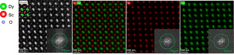
DyScO₃ specimen investigated with the powerful combination of ultra-high brightness X-CFEG, S-CORR, and the large solid angle (1.76 Sr) of the Dual-X detectors, resulting in high signal-to-noise ratio, atomic resolution (up to 90 pm), unfiltered EDS maps (Sample courtesy Professor L.F. Kourkoutis, Cornell University). Image Credit: Thermo Fisher Scientific – Electron Microscopy Solutions
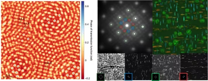
Localized positions of plasmon excitations along a gold nanowire as a function of their excitation energy (between 0.18 – 1.2 eV), investigated with an electron probe of <0.2 eV energy resolution. Image Credit: Thermo Fisher Scientific – Electron Microscopy Solutions
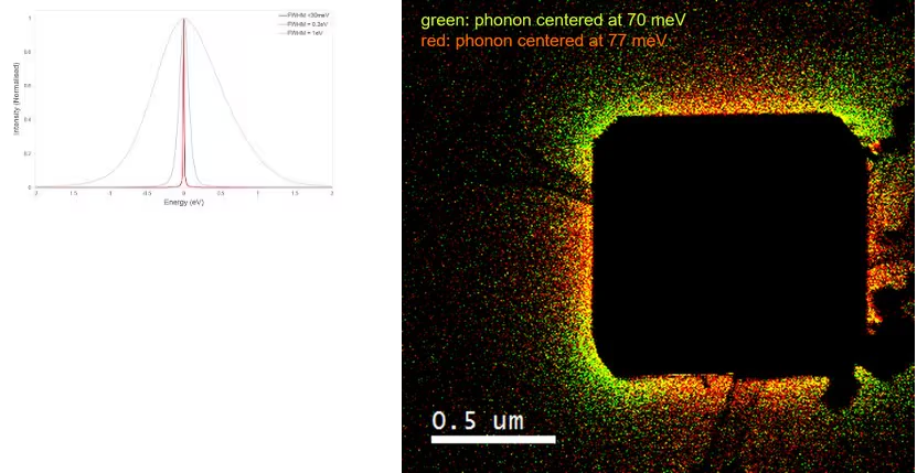
Map of two surface phonons split in energy by 7 meV on a MgO crystal, observed via an electron probe with energy resolution <0.025 eV. Image Credit: Specimen and analysis courtesy of Isobel Bicket and Prof. Gianluigi Botton, The Canadian Centre for Electron Microscopy, McMaster University.
In Situ Capabilities of the Spectra 300 (S)TEM
The Spectra 300 (S)TEM's all-in-one S-TWIN wide-gap pole piece allows it to accept a wide variety of holders for in situ research. For atomic imaging at high temperatures, the Thermo Scientific NanoEx holding family can be easily coupled with the microscope to facilitate MEMS device-based heating.
Below, gold nanoparticles are heated to 700 ºC. The resulting motion is simultaneously recorded on a Thermo Scientific Ceta Camera with speed enhancement at a rate greater than 30 frames per second with full frame 4k by 4k pixel resolution. This results in a high temporal and spatial resolution of extremely dynamic molecular behavior.
Specifications
Source: Thermo Fisher Scientific – Electron Microscopy Solutions
| . |
. |
|
Image corrector
|
- Energy spread: 0.2–0.3 eV
- Information limit: 60 pm
- STEM resolution: 136 pm
|
|
Probe corrector
|
- Energy spread: 0.2–0.3 eV
- Information limit: 100 pm
- STEM resolution: 50 pm (125 pm @ 30 kV)
|
|
Uncorrected
|
- Energy spread: 0.2–0.3 eV
- Information limit: 100 pm
- STEM resolution: 136 pm
|
|
X-FEG/monochromator double corrected (probe+image corrector
|
- Energy spread: 0.2–0.3 eV
- Information limit: 60 pm
- STEM resolution: 50 pm (125 pm @ 30 kV)
|
|
X-CFEG double-corrected (probe+image correction)
|
- Energy spread: 0.4 eV
- Information limit: 70 pm
- STEM resolution: 50 pm (136 pm @ 30 kV)
|
|
Source
|
- X-FEG Mono: High-brightness Schottky field emitter gun and monochromator with a tunable energy resolution range between 1 eV and <0.2 eV
- X-FEG UltiMono: High-brightness Schottky field emitter gun with ultra-stable monochromator and accelerating voltage with a tunable energy resolution range between 1eV and <0.03 eV
- X-CFEG: Ultra-high brightness with an intrinsic energy resolution of <0.4 eV
- Flexible high-tension range from 30 – 300 kV
|